Anti-reflection and self-cleaning glass and manufacturing method thereof
A manufacturing method and self-cleaning technology, which is applied in the field of glass surface processing and micro-nano manufacturing, can solve the problems of being difficult to have anti-reflection and self-cleaning at the same time, poor adaptability to ambient temperature and humidity, and high production costs, and achieve high efficiency and low cost. Advanced production, strong adaptability to harsh environments, and good consistency of embossed graphics
- Summary
- Abstract
- Description
- Claims
- Application Information
AI Technical Summary
Problems solved by technology
Method used
Image
Examples
Embodiment 1
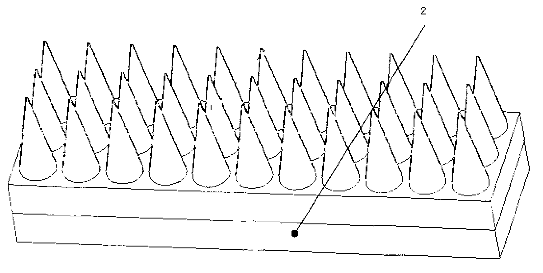
[0055] A subwavelength nano-cone array structure is formed on the exposed glass surface.
[0056] Such as figure 1 As shown, a sub-wavelength nanocone array structure is etched on the exposed glass surface. The shape of the nanocone is conical, the diameter of the bottom surface is 180nm, and the aspect ratio is 4 (the height of the nanocone is 880nm). The center of the bottom surface of the nanocone The pitch (period) between them is 220nm.
[0057] The specific preparation steps are as follows ( Figure 2~3 ):
[0058] (1) Pretreatment
[0059] ① Clean the glass substrate 2, respectively use acetone, ethanol, and deionized water to ultrasonically clean the glass sheet for 5 minutes, blow dry it with nitrogen, and dry it, such as image 3 a;
[0060] 2. Deposit a hard mask layer, and deposit 300nm silicon dioxide on the glass substrate 2 as a hard mask layer, such as image 3 b.
[0061] (2) Liquid imprint material 3 coating
[0062] A slit coating method is used to u...
Embodiment 2
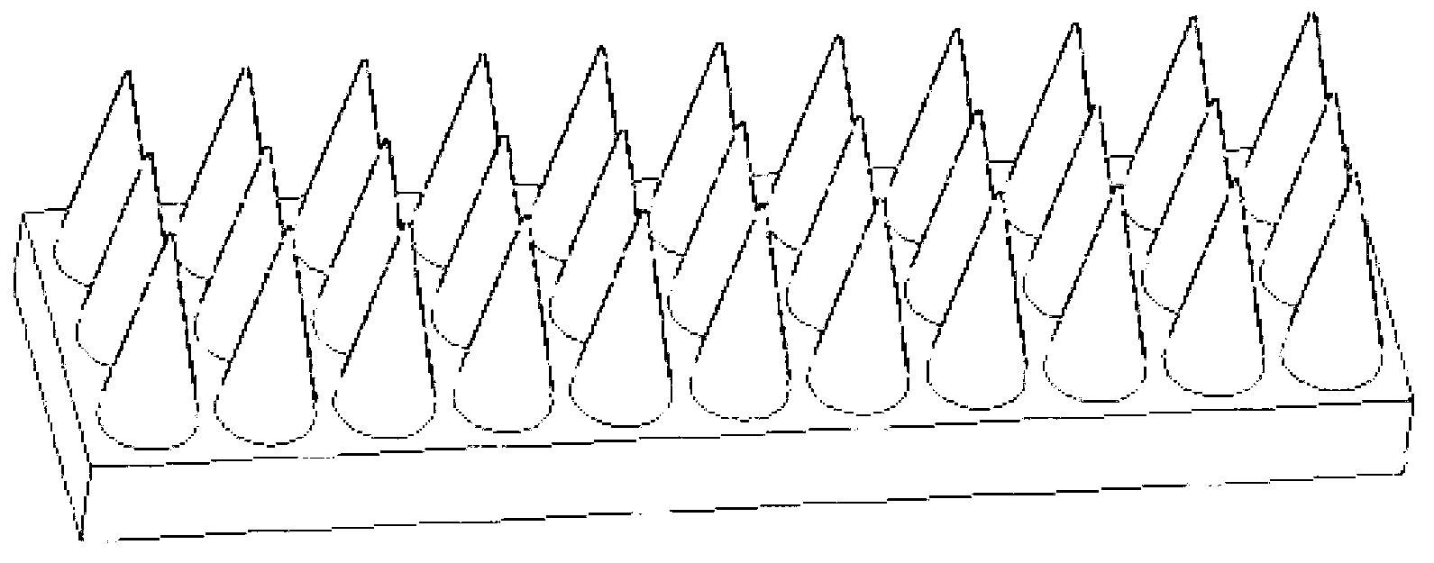
[0078] The sub-wavelength nano-cone array structure is directly imprinted on the liquid imprint material coating of the glass substrate.
[0079] Such as Figure 5 As shown, the surface of the glass substrate 2 is coated with a coating of liquid imprinting material, and a sub-wavelength nano-cone array structure is directly imprinted on the coating. The aspect ratio is 5 (the height of the nanocones is 1000nm), and the spacing (period) between the centers of the bottom surfaces of the nanocones is 260nm.
[0080] The coating described in this example is a nano-titanium dioxide-based UV-curable transparent liquid imprinting material (such as an imprinting material formed by adding titanium dioxide nanoparticles to an epoxy polymer matrix KATIONBOND OMVE 110707).
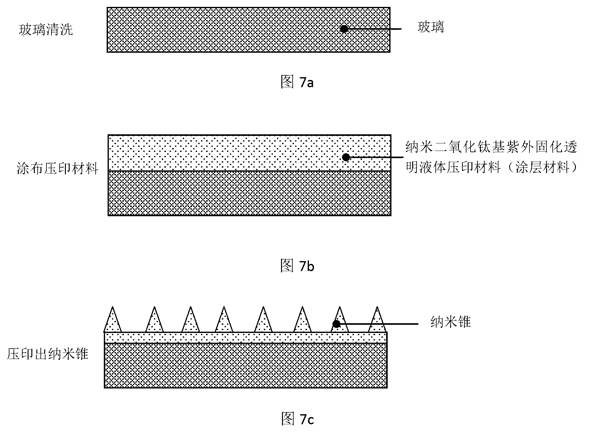
[0081] Specific steps are as follows( Figure 6~7 ):
[0082] (1) Pretreatment
[0083] ① The glass substrate 2 is cleaned, and the glass sheet is ultrasonically cleaned with acetone, ethanol, and deionized water ...
PUM
 Abstract
Description
Claims
Application Information


