Efficient triple-junction solar cell and manufacturing method thereof

A solar cell and manufacturing method technology, applied in circuits, photovoltaic power generation, electrical components, etc., can solve the problems of limited conversion rate of solar cells, complex flip-chip growth process, affecting cell efficiency, etc., to reduce dark current and reduce fragmentation rate. , spectral absorption and reasonable effect

Inactive Publication Date: 2013-08-21
XIAMEN SANAN OPTOELECTRONICS TECH CO LTD
View PDF3 Cites 9 Cited by
  • Summary
  • Abstract
  • Description
  • Claims
  • Application Information

AI Technical Summary

Problems solved by technology

The commonly used candidate material is In0.3Ga0.7As (1eV), but its lattice constant does not match the GaAs substrate or Ge substrate, in order to overcome this crystal Lattice mismatch is introduced into the graded buffer layer, but the crystal quality of the graded buffer layer greatly affects the cell efficiency
The Chinese patent application publication "A high-efficiency triple-junction solar cell with current matching and lattice matching" (application number CN200910019869.X) proposes to use a strain-compensated superlattice as a subcell to achieve current matching and lattice matching, but The energy bandgap distribution of each sub-cell is 1.65~1.75eV / 1.0eV / 0.67eV, which is only the second best choice for capturing the solar spectrum. The conversion rate of solar cells is limited, and the expensive Ge substrate is used, and the cost is high.
Emcore Solar Power, Inc. proposed a flip-chip deformed multi-junction solar cell InGaP / GaAs / InGaAs, which satisfies the above energy bandgap distribution, but the flip-chip growth process is complicated, and the subsequent process is more complicated, which greatly limits application of this technology in industry

Method used


Image

  • Efficient triple-junction solar cell and manufacturing method thereof

Examples


Embodiment 1

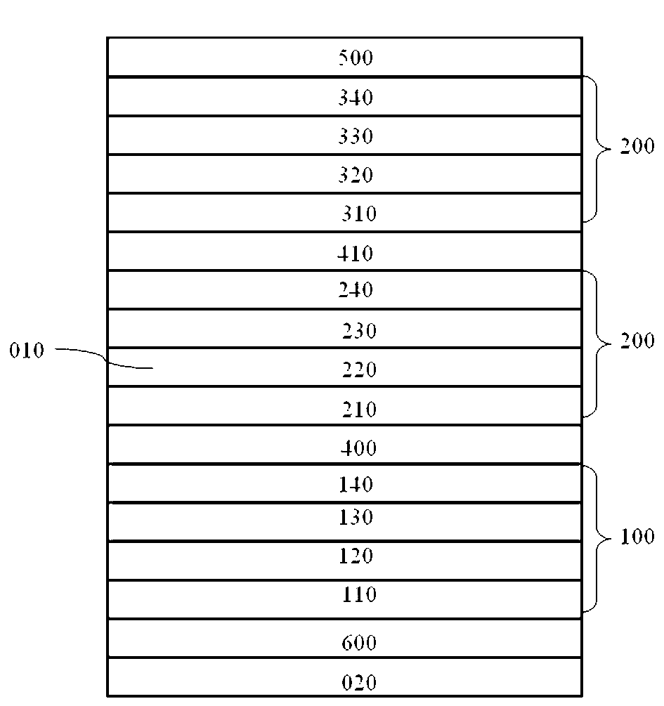
[0021] figure 1 It is a schematic structural diagram of a high-efficiency triple-junction solar cell implemented according to the present invention.

[0022] Such as figure 1 As shown, a high-efficiency triple-junction solar cell includes a support substrate 020, a DBR reflective layer 600, a bottom cell 100, a middle cell 200, a top cell 300, a highly doped capping layer 500, and tunnel junctions between each junction cell. 410, 420 connections. Wherein, the bottom cell 100 is grown upside down on the back side of the growth substrate 010, the middle cell uses the growth substrate 010 itself as the base region 220, the emitter region 230 is epitaxially grown on the front side of the growth substrate, and the top cell is formed on the middle cell . The specific structure thereof is described in detail below.

[0023] The growth substrate 010 is an ultra-thin substrate that has been polished on both sides. In the present invention, in this implementation, a p-type GaAs sub...

Embodiment 2

[0039] This embodiment is a manufacturing process of a high-efficiency triple-junction solar cell described in Example 1, which includes the formation process of the sub-cells 100, 200, 300, and layers between the sub-cells.

[0040] Concrete preparation process comprises the following steps:

[0041] In the first step, a growth substrate 010 is provided. The growth substrate 010 is an ultra-thin substrate that has been polished on both sides. In this implementation, a p-type GaAs substrate with a thickness of about 200 microns is selected, and its doping concentration is 2×10 17 cm -3 ~5×10 17 cm -3 .

[0042] In the next step, a neutron pool 020 is formed on the front surface of the growth substrate 010 with a band gap of 1.4-1.5eV. The specific process is as follows: In the MOCVD system, the above-mentioned GaAs substrate 010 polished on both sides is used as the base region 220 of the battery, and the n-type emitter region 230 is epitaxially grown on the...


PUM


Abstract

The invention discloses an efficient triple-junction solar cell and a manufacturing method thereof. The efficient triple-junction solar cell comprises a growth substrate, a bottom cell, an intermediate cell and a top cell, wherein the growth substrate is provided with two polished surfaces; the bottom cell is formed by a strain compensation superlattice structure, grows on the reverse side of the growth substrate in an inverted mode, and is provided with a first band gap, and the equivalent lattice constant of the bottom cell is matched with that of the growth substrate; the intermediate cell is formed on the obverse side of the growth substrate and is provided with a second band gap larger than the first band gap, and the lattice constant of the intermediate cell is matched with that of the growth substrate; the top cell is formed on the intermediate cell and provided with a third bang gap larger than the second band gap, and the lattice constant of the top cell is matched with that of the intermediate cell. Distribution of energy band gaps of the triple-junction solar cell meets an optimal choice for capturing a solar energy spectrum, and current matching and lattice matching are achieved, so photoelectric conversion efficiency of the triple-junction solar cell is effectively improved; according to the manufacturing method of the triple-junction solar cell, a mode of double-faced growth on the growth substrate is adopted, so growth cockamamie processes brought in the later stage of inverted growth are eliminated, and the yield of products is improved.

Description

technical field [0001] The invention relates to a high-efficiency strain-compensated triple-junction solar cell and a manufacturing method thereof, belonging to the technical field of semiconductor materials. Background technique [0002] In recent years, solar cells have attracted more and more attention as a practical new energy source. It is a semiconductor device that uses the photovoltaic effect to convert solar energy into electrical energy, which greatly reduces people's dependence on coal, oil and natural gas in production and life, and has become one of the most effective ways to use green energy. With the development of concentrated photovoltaic technology, III-V compound semiconductor solar cells have attracted more and more attention because of their high photoelectric conversion efficiency. [0003] At present, one of the main obstacles restricting the development of the III-V compound semiconductor solar cell industry is the high cost of its components, which ...

Claims


Application Information

Patent Timeline
Patent Type & Authority Applications(China)
IPC IPC(8): H01L31/0352H01L31/078H01L31/0304H01L31/18
CPCH01L31/06875H01L31/1892Y02E10/544
Inventor 毕京锋林桂江刘建庆王良均熊伟平宋明辉
Owner XIAMEN SANAN OPTOELECTRONICS TECH CO LTD
Why Eureka
Try Eureka