
A kind of preparation method of organic thin film transistor

An organic thin film and transistor technology, applied in the field of organic thin film transistor preparation, can solve the problems of limiting the application of rubrene, it is difficult to obtain hole mobility, and it is difficult to form a highly ordered crystalline film, so as to improve the π-π The effect of improving carrier transfer efficiency and improving carrier transport efficiency

Inactive Publication Date: 2015-10-21
CHONGQING UNIV
View PDF3 Cites 0 Cited by
  • Summary
  • Abstract
  • Description
  • Claims
  • Application Information

AI Technical Summary

Problems solved by technology

The organic semiconductor devices prepared by rubrene single crystals have always maintained a high field-effect mobility (15~40 cm2 / V s), but single crystals of this size, thickness and shape Transistor devices are difficult to control the fabrication process
Therefore, many people are committed to preparing rubrene organic thin film transistors by vacuum vapor deposition, but it is difficult to obtain ideal hole mobility for rubrene organic thin film transistors prepared by vacuum vapor deposition, mainly because During the process, it is difficult for rubrene to form a highly ordered crystalline film, which greatly limits the application of rubrene in organic semiconductor devices.

Method used


Image

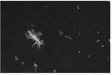
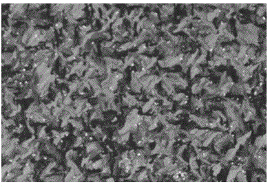
  • A kind of preparation method of organic thin film transistor
  • A kind of preparation method of organic thin film transistor
  • A kind of preparation method of organic thin film transistor

Examples


Embodiment 1

[0018] First step SiO 2 / Si substrate pretreatment: the cut SiO 2 / Si substrate was ultrasonically cleaned in acetone for 10 minutes, dried with a nitrogen gun and then placed in H 2 SO 4 (98%): H 2 o 2 (30%) = 7:3 solution, treated at 100°C for 1 hour; take it out, wash it with deionized water, dry it with a nitrogen gun, and place it in NH 3 (30%): H 2 o 2 (30%): H 2 O=1:1:5 solution, treated at 70°C for 20 minutes, cleaned with deionized water after taking it out, blown dry with nitrogen gun, and the cleaning of the substrate was completed;

[0019] The second step is vacuum evaporation of rubrene to form a film: the above pretreated SiO 2 / Si substrate is placed in a vacuum evaporation apparatus, and the vacuum pressure is 1×10 -4 Under Pa, the substrate temperature is 25°C-110°C to evaporate 80nm rubrene (four parallel experiments are 25°C, 60°C, 90°C, 110°C), and the evaporation rate is 2~4 nm / min;

[0020] Step 3 Vacuum evaporation of metal electrodes: Evapo...

Embodiment 2

[0024] SiO 2 / Si substrate pretreatment, as embodiment 1;

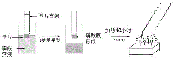
[0025] Self-assembly treatment of the substrate: Dissolve n-octadecylphosphoric acid in tetrahydrofuran to prepare a 1mmol / L solution, such as figure 2 As shown, using the pulling method (the so-called pulling method is to make the solvent evaporate naturally on SiO 2 / Si substrate to form a uniform film, grown n-octadecyl phosphate film) in the pretreated SiO 2 N-octadecyl phosphoric acid film was grown on the Si substrate, and reacted in a vacuum oven at 140°C for 48 hours. During this process, the phosphoric acid film formed a stable chemical bond with the silicon dioxide surface; then it was taken out and cleaned with tetrahydrofuran ultrasonically. SiO 2 / Si substrate for 5 minutes, the substrate after cleaning is smooth and smooth, and a uniformly distributed n-octadecyl phosphoric acid layer can be seen under the atomic force microscope, with a thickness of 2.4~4.8 nm;

[0026] Vacuum evaporation of organi...

Embodiment 3

[0031] SiO 2 / Si substrate pretreatment, as embodiment 1;

[0032] The self-assembly process of substrate, as embodiment 2;

[0033] Vacuum evaporation organic template layer: the above self-assembled substrate with n-octadecyl phosphoric acid film is placed in a vacuum evaporation apparatus, and the vacuum pressure is 6.0×10 -5 Under Pa, at a substrate temperature of 60°C, vapor-deposit a 5nm layer of 6,13-pentacenepyrazine (DAP) molecules at a speed of 2-4 nm / min;

[0034] Vacuum deposition of rubrene: rubrene is deposited without opening the vacuum chamber, the substrate temperature is 90°C, and 80nm rubrene is thermally deposited as the semiconductor layer;

[0035] Vacuum evaporation of metal electrodes was carried out as in Example 1, and a rubrene organic thin film transistor device was prepared.

[0036]The rubrene organic thin film transistor prepared by evaporating DAP at a substrate temperature of 60°C shows a hole transport performance of 6.8×10 -1 cm 2 / V·s...


PUM

PropertyMeasurementUnit
Thicknessaaaaaaaaaa
Thicknessaaaaaaaaaa

Abstract

The invention discloses a preparation method of an organic thin film transistor. The preparation method of the organic thin film transistor includes the steps of carrying pre-processing of a SiO2 / Si substrate, carrying out self-assembly processing of the substrate, carrying out vacuum evaporation on an organic formwork layer, then evaporating a 80nm rubrene layer at the substrate temperature of 25-110 DEG C and finally carrying out vacuum evaporation on a gold electrode to obtain a rubrene organic thin film transistor component. The self-assembly processing of the substrate includes the following steps: dissolving octadecylphosphonic acid into tetrahydrofuran (THF) to prepare a 1mmol / L solution, and growing an octadecylphosphonic acid film on the pre-processed SiO2 / Si substrate with the czochralski method. The vacuum evaporation on the organic formwork layer includes the following steps: placing the substrate provided with the octadecylphosphonic acid film in a self-assembling mode in a vacuum evaporation apparatus, and evaporating a 5-15nm 6,13-pentacene pyrazine (DAP) molecular layer at the vacuum pressure smaller than 1*10<-4>Pa and at the substrate temperature of 25-80 DEG C. The preparation method of the organic thin film transistor has the advantages of being capable of obtaining the orderly crystal-shaped rubrene organic thin film, and promoting carrier transferring efficiency of the rubrene organic thin film transistor.

Description

technical field [0001] The invention belongs to a method for preparing a transistor, and in particular relates to a method for preparing an organic thin film transistor. Background technique [0002] Organic thin film transistors (OTFTs) are low-cost electronic devices used in electronic price tags, smart cards, flexible electronic paper, backplane circuits in active matrix displays, and organic solar cell devices. Organic semiconductor devices prepared from rubrene single crystals have always maintained high field-effect mobility (15-40 cm 2 / V·s), but it is difficult to control the manufacturing process of single crystal transistor devices of this size, thickness and shape. Therefore, many people are committed to preparing rubrene organic thin film transistors by vacuum vapor deposition, but it is difficult to obtain ideal hole mobility for rubrene organic thin film transistors prepared by vacuum vapor deposition, mainly because During the process, it is difficult for ru...

Claims


Application Information

Patent Timeline
IPC IPC(8): H01L51/40
Inventor 李哲峰李娇
Owner CHONGQING UNIV
Learn More