Method of forming opening

A patterned, gas technology, applied in the direction of electrical components, semiconductor/solid-state device manufacturing, circuits, etc., can solve the problems of the influence of the electrical performance of the semiconductor device, the damage of the inner wall of the opening, etc.

Active Publication Date: 2013-10-30
SEMICON MFG INT (SHANGHAI) CORP
View PDF9 Cites 11 Cited by
  • Summary
  • Abstract
  • Description
  • Claims
  • Application Information

AI Technical Summary

Problems solved by technology

[0004] In the process of etching the dielectric layer 3 to form a dual damascene opening in the existing process, since the material of the dielectric layer 3 is a low-k material or an ultra-low-k material, damage 8 is easily caused to the inner wall of the opening, and the metal conductive layer exposed by the opening The surface will a

Method used


Image

  • Method of forming opening
  • Method of forming opening
  • Method of forming opening

Examples


Embodiment 1

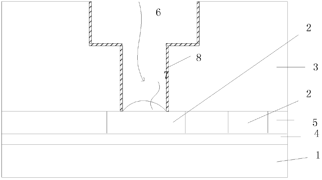
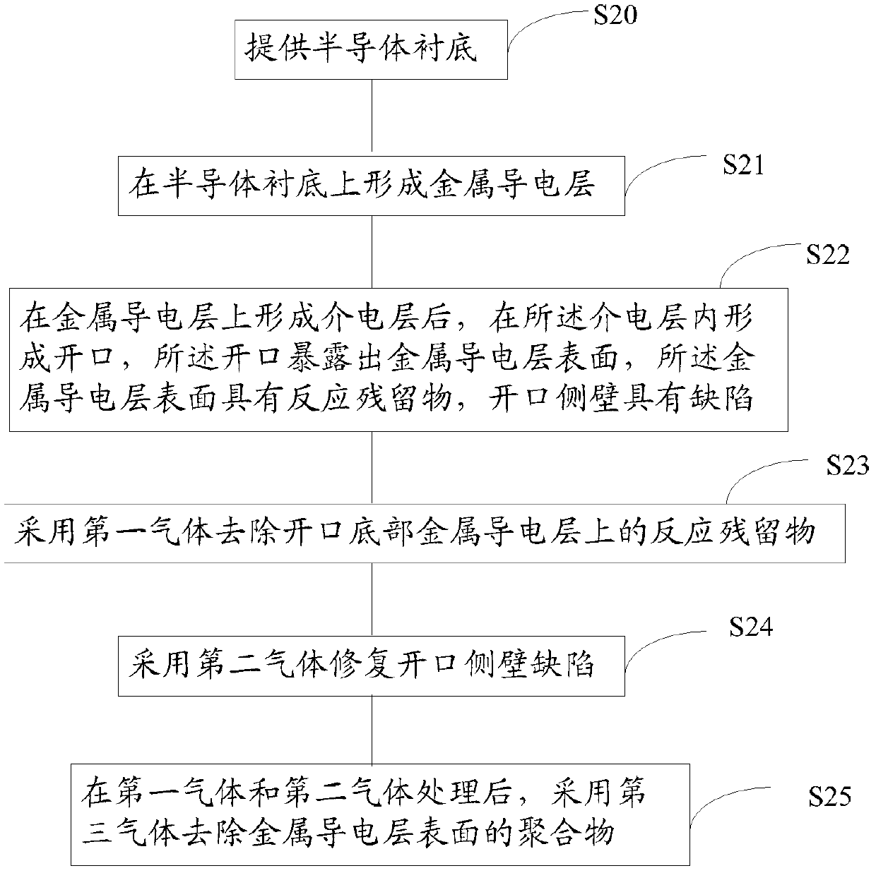
[0048] Figure 3 to Figure 14 It is a schematic diagram of an embodiment of forming a dual damascene structure with openings in the first embodiment of the present invention.

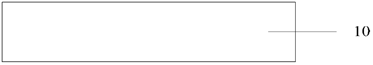
[0049] like image 3 As shown, a semiconductor substrate 10 is provided, and the semiconductor substrate 10 may be a monocrystalline silicon (monocrystalline) substrate or a silicon on insulator (silicon on insulator) substrate. Of course, it can also be other substrate materials known to those skilled in the art. Wherein, semiconductor elements, such as transistors, capacitors, rectifiers, etc., may have been formed on the semiconductor substrate 10 .

[0050] like Figure 4 As shown, a first interlayer dielectric layer 11 is formed on a semiconductor substrate 10 formed with semiconductor devices.

[0051] In this embodiment, the process for forming the first interlayer dielectric layer 11 may be chemical vapor deposition (CVD), physical vapor deposition (PVD), etc.; the material of the first inte...

Embodiment 2

[0083] The difference between the second embodiment and the above embodiment is that before forming the first patterned photoresist layer, a patterned hard mask layer can also be formed on the dielectric layer, and the patterned hard mask layer is used Where the trenches are defined, the photoresist layer is patterned to define the via hole locations, and then the remaining photoresist layer and hard mask layer are removed. details as follows:

[0084] Firstly, a semiconductor substrate is provided; a metal conductive layer is formed on the semiconductor substrate; a dielectric layer is formed on the metal conductive layer, please refer to the first embodiment for details.

[0085] Next, a hard mask layer is formed on the dielectric layer.

[0086] The hard mask layer may be formed of common hard mask materials, such as silicon oxide, silicon nitride, silicon oxynitride, and silicon carbide. However, as the size of semiconductor devices continues to shrink, it becomes more a...

Embodiment 3

[0092] In the above embodiment, the first gas to the third gas are used to perform post-etching treatment on the dual damascene openings. In the third embodiment, the first gas to the third gas are used to directly perform post-etching treatment to the via holes in the dielectric layer.

[0093] like Figure 15 As shown, a semiconductor substrate 40 is provided, please refer to the first embodiment for details.

[0094] like Figure 16 As shown, a first interlayer dielectric layer 41 is formed on a semiconductor substrate 40 formed with semiconductor devices; a discrete metal conductive layer 42 is formed on the first interlayer dielectric layer 41, and the metal conductive layer 42 passes through the first interlayer dielectric layer 41. The conductive structure in the interlayer dielectric layer 41 is connected to the semiconductor element on the semiconductor substrate 40; the second interlayer dielectric layer 43 is formed on the first interlayer dielectric layer 41 betwe...


PUM


Abstract

Disclosed is a method of forming an opening. The method comprises the steps of providing a semiconductor substrate; forming a metal conductive layer on the semiconductor substrate; forming a dielectric layer on the metal conductive layer and forming an opening in the dielectric layer with the opening exposing a surface of the metal conductive layer, the surface of the metal conductive layer having a reaction residue and a side wall of the opening having a defect; removing the reaction residue on the metal conductive layer at the bottom of the opening by use of a first gas; repairing the defect on the side wall of the opening by use of a second gas; and removing, after treatment of the first gas and the second gas, a polymer on the surface of the metal conductive layer by use of a third gas. The method of forming the opening is used for improving electrical properties, stability and yield of an integrated circuit.

Description

technical field [0001] The invention relates to the field of semiconductor manufacturing, in particular to a method for forming an opening. Background technique [0002] With the continuous development of semiconductor integrated circuit technology, the size of semiconductor devices and the size of interconnection structures are continuously reduced, resulting in the gradual reduction of the spacing between metal wirings, and the dielectric layer used to isolate metal wirings has also become It is getting thinner and thinner, which may cause crosstalk between metal lines. Now, this crosstalk can be effectively reduced by lowering the dielectric constant (k) of the dielectric layer between the metal wiring layers. The dielectric layer of low-k material can effectively reduce the resistance-capacitance delay (RC delay) between metal wiring layers. Therefore, low-k dielectric materials and ultra-low-k dielectric materials have been more and more widely used in the dielectric ...

Claims


Application Information

Patent Timeline
IPC IPC(8): H01L21/311H01L21/768
Inventor 张海洋胡敏达周俊卿
Owner SEMICON MFG INT (SHANGHAI) CORP
Why Eureka
Try Eureka