

Lateral direction SOI power semiconductor device
A technology of power semiconductors and semiconductors, which is applied to semiconductor devices, electrical components, circuits, etc., can solve problems such as high cost, difficult manufacturing process, and substrate auxiliary depletion, so as to reduce on-resistance, manufacturing process difficulty and cost Low, improve the effect of breakdown voltage
- Summary
- Abstract
- Description
- Claims
- Application Information
AI Technical Summary
Problems solved by technology
Method used
Image

Examples
Embodiment Construction
[0030] The present invention will be described in detail below in conjunction with the accompanying drawings.
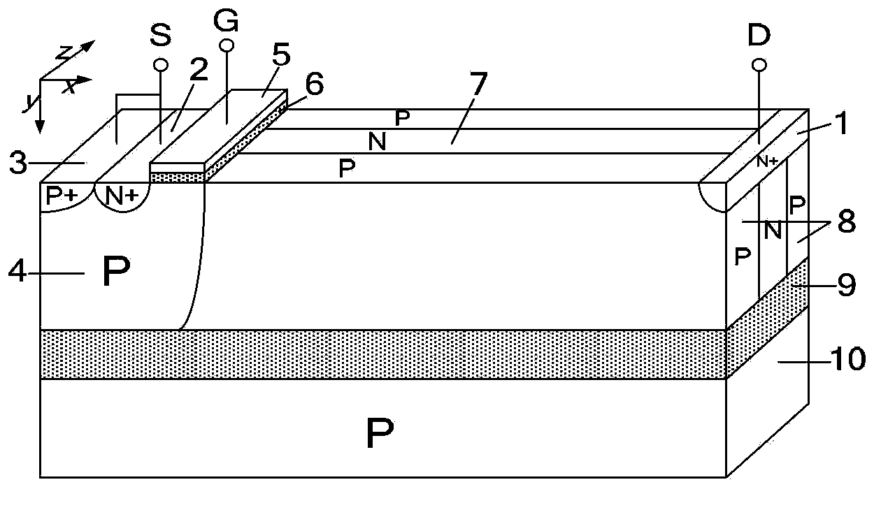
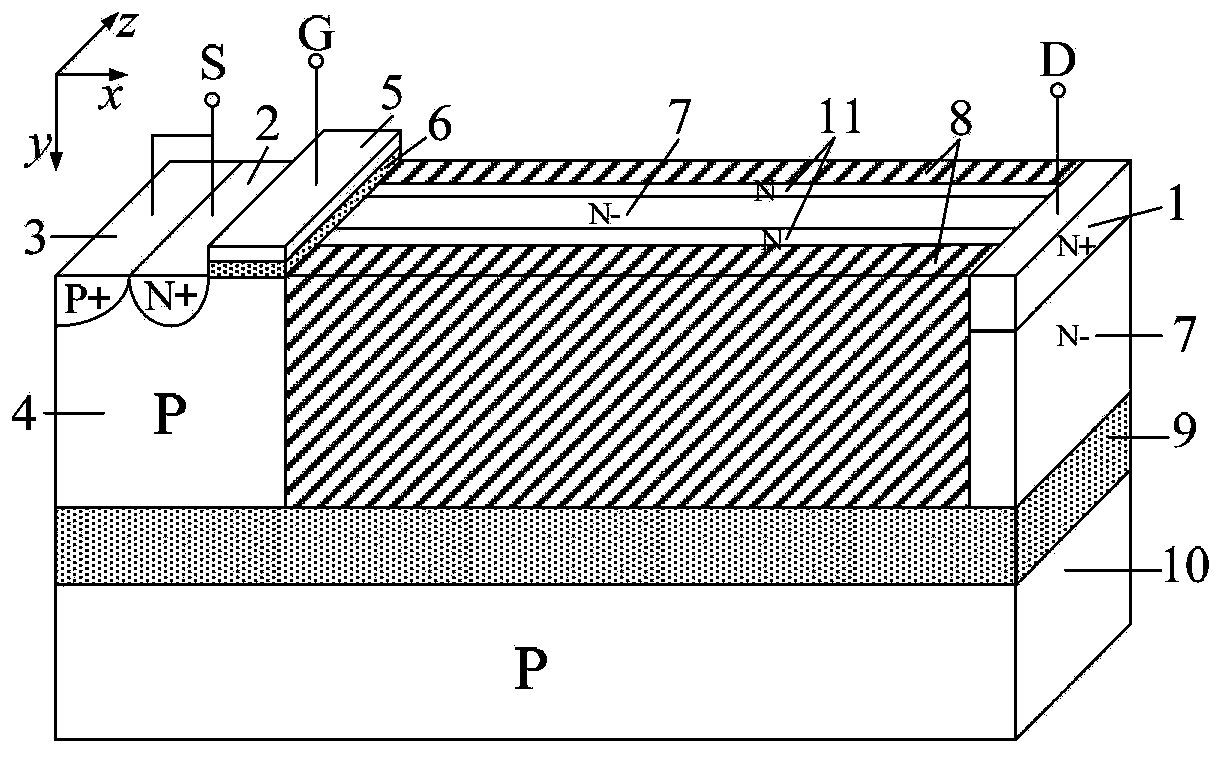
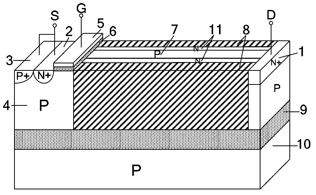
[0031] Conventional superjunction SOI LDMOS structure, such as figure 1 As shown, 10 is a P-type semiconductor substrate layer. 9 is a silicon dioxide insulating dielectric layer located above the substrate layer 10 . One end above the silicon dioxide insulating dielectric layer 9 is a P-type body region 4 , the surface of the body region 4 is a P-type body contact region 3 and an N-type source region 2 in sequence, and the source electrode S is drawn from the surface of the body contact region 3 and the source region 2 . Above the body region 4 is a gate dielectric 6, preferably, the gate dielectric 6 is silicon dioxide, and above the gate dielectric 6 is a conductive material 5, preferably, the conductive material 5 is formed of polysilicon, and a gate electrode G is drawn from the conductive material 5.
[0032] 7 is an N-type drift region, and there is a P-typ...
PUM
 Abstract
Description
Claims
Application Information