

Method for preparing er-doped silicon carbide optical waveguide through ion implantation
A silicon carbide optical and ion implantation technology, applied in the direction of light guides, optics, optical components, etc., can solve the problems of low activation efficiency, secondary defects, and restrictions on erbium-doped silicon carbide optical waveguides, so as to avoid low waveguide gain and improve Effects of light gain and enhancement of fluorescence luminous efficiency
- Summary
- Abstract
- Description
- Claims
- Application Information
AI Technical Summary
Problems solved by technology
Method used
Image

Examples
Embodiment 1
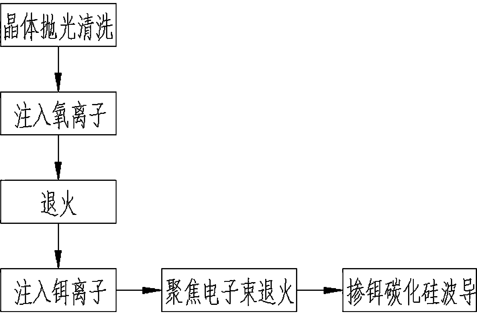
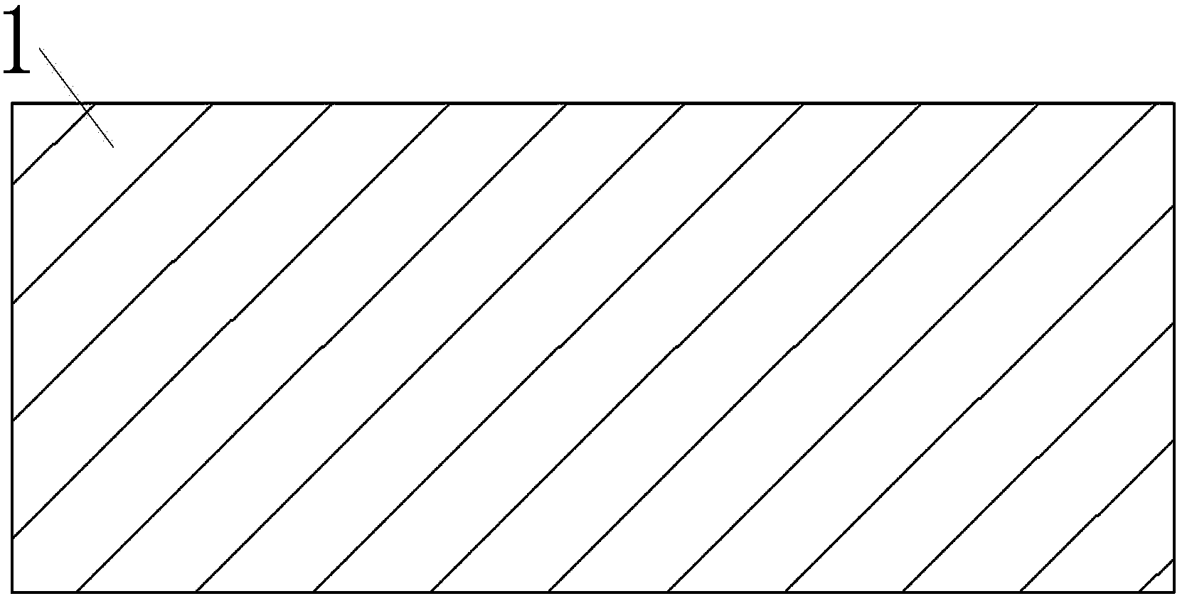
[0028] (1) The silicon carbide sample 1 that has been cut and optically polished is cleaned with acetone and ultrasonic waves, and then the cleaned silicon carbide sample 1 is cleaned.
[0029] (2) Put the sample cleaned in (1) in the target chamber of the accelerator, and evacuate to 1×10 Pa, the implantation process of oxygen ions is performed. The injection energy is 0.5MeV, and the injection dose is 1×10 ions / cm , the whole process is carried out at a temperature of 600°C.
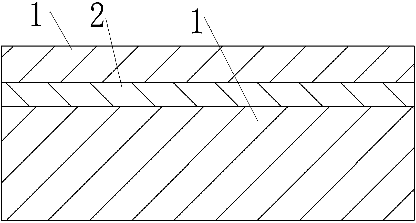
[0030] (3) Place the sample obtained in (2) in an annealing furnace, and perform high-temperature annealing treatment on the sample in an argon atmosphere. The annealing temperature is controlled at 1200°C, and the annealing time is 0.5h. Through this process, a silicon dioxide buried layer 2 with a thickness of approximately 600 nm and a near-stoichiometric ratio can be obtained on the silicon carbide sample.
[0031] (4) Place the sample obtained in (3) in the target chamber of the accelerato...
Embodiment 2
[0036] (1) The silicon carbide sample 1 that has been cut and optically polished is cleaned with acetone and ultrasonic waves, and then the cleaned silicon carbide sample 1 is cleaned.
[0037] (2) Put the sample cleaned in (1) in the target chamber of the accelerator, and evacuate to 1×10 Pa, the implantation process of oxygen ions is performed. The injection energy is 1MeV, and the injection dose is 2.5×10 ions / cm , the whole process is carried out at a temperature of 650°C.
[0038] (3) Place the sample obtained in (2) in an annealing furnace, and perform high-temperature annealing treatment on the sample in an argon atmosphere. The annealing temperature is controlled at 1200° C., and the annealing time is 1 h. A nearly stoichiometric silicon dioxide buried layer 2 with a thickness of about 970 nm can be obtained on the silicon carbide sample through this process.
[0039] (4) Place the sample obtained in (3) in the target chamber of the accelerator, and evacuate to...
Embodiment 3
[0043] (1) The silicon carbide sample 1 that has been cut and optically polished is cleaned with acetone and ultrasonic waves, and then the cleaned silicon carbide sample 1 is cleaned.
[0044] (2) Put the sample cleaned in (1) in the target chamber of the accelerator, and evacuate to 1×10 Pa, the implantation process of oxygen ions is performed. The injection energy is 2.0MeV, and the injection dose is 2.5×10 ions / cm , the whole process is carried out at a temperature of 650°C.
[0045] (3) Place the sample obtained in (2) in an annealing furnace, and perform high-temperature annealing treatment on the sample in an argon atmosphere. The annealing temperature is controlled at 1200° C., and the annealing time is 1 h. Through this process, a silicon dioxide buried layer 2 with a thickness of approximately 600 nm and a near-stoichiometric ratio can be obtained on the silicon carbide sample.
[0046] (4) Place the sample obtained in (3) in the target chamber of the acceler...
PUM
| Property | Measurement | Unit |
|---|---|---|
| Diameter | aaaaa | aaaaa |
| Thickness | aaaaa | aaaaa |
| Thickness | aaaaa | aaaaa |
Abstract
Description
Claims
Application Information