

A method for preparing erbium-doped silicon carbide optical waveguide by ion implantation
A silicon carbide optical and ion implantation technology, applied in the directions of light guides, optics, optical components, etc., can solve the problems of secondary defects, low activation efficiency, restricting erbium-doped silicon carbide optical waveguides, etc., to improve optical gain and enhance fluorescence. Luminous efficiency, avoiding the effect of low waveguide gain
- Summary
- Abstract
- Description
- Claims
- Application Information
AI Technical Summary
Problems solved by technology
Method used
Image

Examples
Embodiment 1
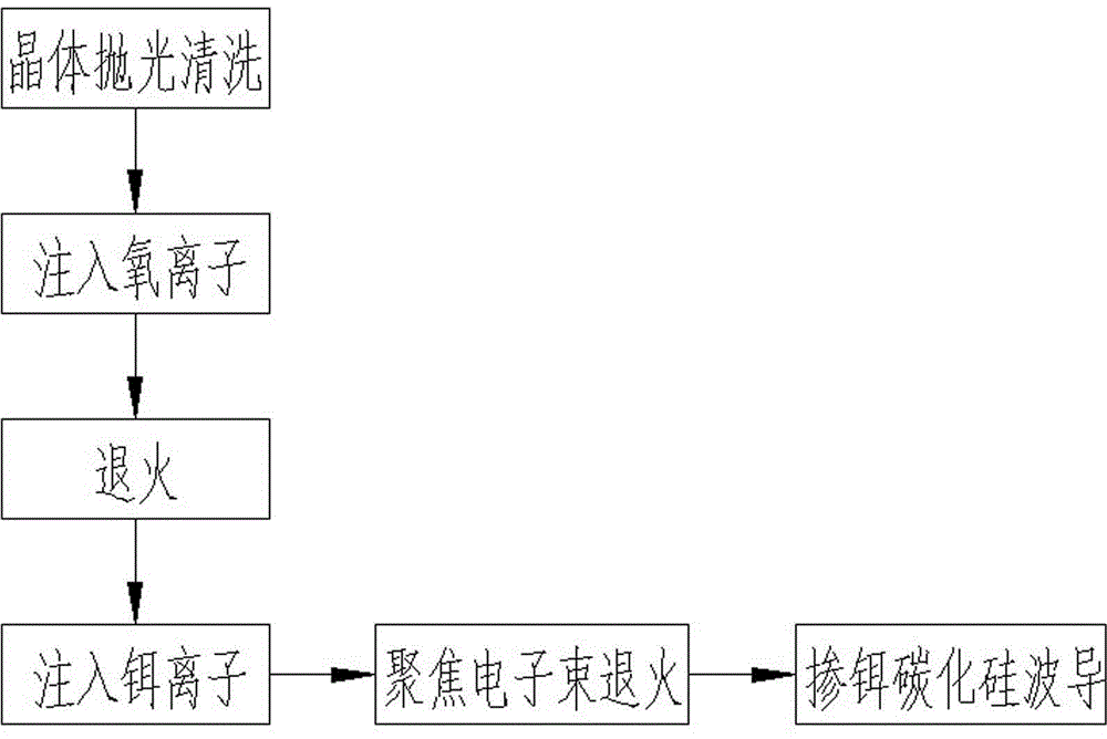
[0028] (1) The silicon carbide sample 1 that has been cut and optically polished is cleaned with acetone and ultrasonic waves, and then the cleaned silicon carbide sample 1 is cleaned.
[0029] (2) Put the sample cleaned in (1) in the target chamber of the accelerator, and evacuate to 1×10 Pa, the implantation process of oxygen ions is performed. The injection energy is 0.5MeV, and the injection dose is 1×10 ions / cm , the whole process is carried out at a temperature of 600°C.
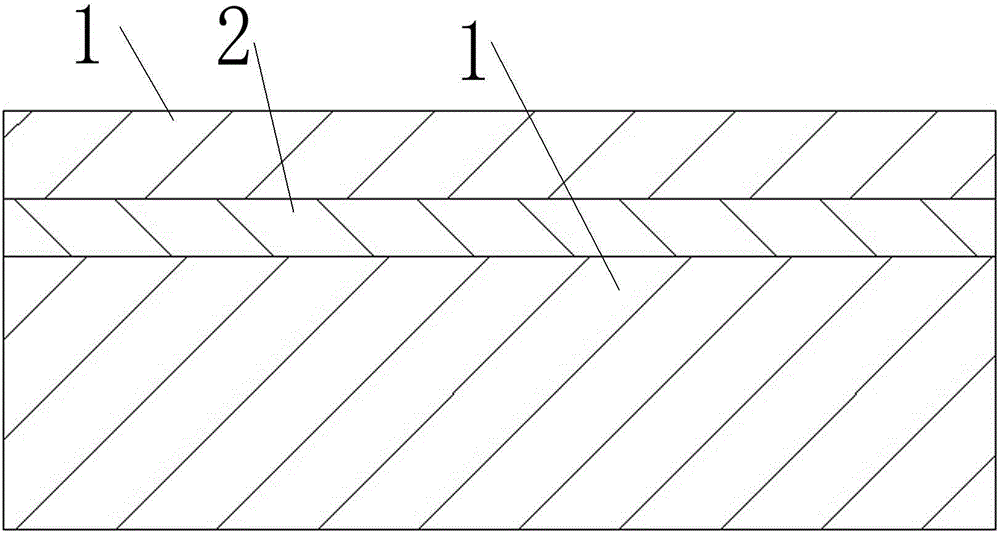
[0030] (3) Place the sample obtained in (2) in an annealing furnace, and perform high-temperature annealing treatment on the sample in an argon atmosphere. The annealing temperature is controlled at 1200°C, and the annealing time is 0.5h. Through this process, a silicon dioxide buried layer 2 with a thickness of approximately 600 nm and a near-stoichiometric ratio can be obtained on the silicon carbide sample.
[0031] (4) Place the sample obtained in (3) in the target chamber of the accelerato...
Embodiment 2
[0035] (1) The silicon carbide sample 1 that has been cut and optically polished is cleaned with acetone and ultrasonic waves, and then the cleaned silicon carbide sample 1 is cleaned.
[0036] (2) Put the sample cleaned in (1) in the target chamber of the accelerator, and evacuate to 1×10 Pa, the implantation process of oxygen ions is performed. The injection energy is 1MeV, and the injection dose is 2.5×10 ions / cm , the whole process is carried out at a temperature of 650°C.
[0037] (3) Place the sample obtained in (2) in an annealing furnace, and perform high-temperature annealing treatment on the sample in an argon atmosphere. The annealing temperature is controlled at 1200° C., and the annealing time is 1 h. A nearly stoichiometric silicon dioxide buried layer 2 with a thickness of about 970 nm can be obtained on the silicon carbide sample through this process.
[0038] (4) Place the sample obtained in (3) in the target chamber of the accelerator, and evacuate to...
Embodiment 3
[0042] (1) The silicon carbide sample 1 that has been cut and optically polished is cleaned with acetone and ultrasonic waves, and then the cleaned silicon carbide sample 1 is cleaned.
[0043] (2) Put the sample cleaned in (1) in the target chamber of the accelerator, and evacuate to 1×10 Pa, the implantation process of oxygen ions is performed. The injection energy is 2.0MeV, and the injection dose is 2.5×10 ions / cm , the whole process is carried out at a temperature of 650°C.
[0044] (3) Place the sample obtained in (2) in an annealing furnace, and perform high-temperature annealing treatment on the sample in an argon atmosphere. The annealing temperature is controlled at 1200° C., and the annealing time is 1 h. Through this process, a silicon dioxide buried layer 2 with a thickness of approximately 600 nm and a near-stoichiometric ratio can be obtained on the silicon carbide sample.
[0045] (4) Place the sample obtained in (3) in the target chamber of the acceler...
PUM
| Property | Measurement | Unit |
|---|---|---|
| diameter | aaaaa | aaaaa |
| depth | aaaaa | aaaaa |
| thickness | aaaaa | aaaaa |
Abstract
Description
Claims
Application Information