Method for manufacturing copper indium gallium diselenide thin-film solar cells

A solar cell, copper indium gallium selenide technology, which is applied to conductive materials, circuits, electrical components and other directions dispersed in non-conductive inorganic materials, can solve problems such as increasing cost and affecting appearance, and achieves convenient high-temperature processing and reduces manufacturing costs. , the effect of simple process

Inactive Publication Date: 2013-12-25
XIAMEN UNIV +1
View PDF6 Cites 5 Cited by
  • Summary
  • Abstract
  • Description
  • Claims
  • Application Information

AI Technical Summary

Problems solved by technology

At present, BIPV mainly integrates silicon-based and other solar panels on the surface of buildings such as roofs. This method will not only increase additional costs, but also affect the appearance.

Method used


Image

  • Method for manufacturing copper indium gallium diselenide thin-film solar cells
  • Method for manufacturing copper indium gallium diselenide thin-film solar cells
  • Method for manufacturing copper indium gallium diselenide thin-film solar cells

Examples


Embodiment 1

[0032] Mix 7g molybdenum powder (particle size 0.01-50μm), 0.5g glass powder (lead-free glass powder), 0.5g terpineol, 1g polyethylene glycol-200, 0.25g polyethylene glycol-400, 0.1g epoxy Resin E44 (or E51), 0.005g NaOH, 0.1g ethyl cellulose, 0.01g dibutyl phthalate, 0.03g Span 85 (sorbitan trioleate), 0.5g ethanol, 0.005g silicone oil Put them together and mix evenly to prepare a composite conductive molybdenum paste.

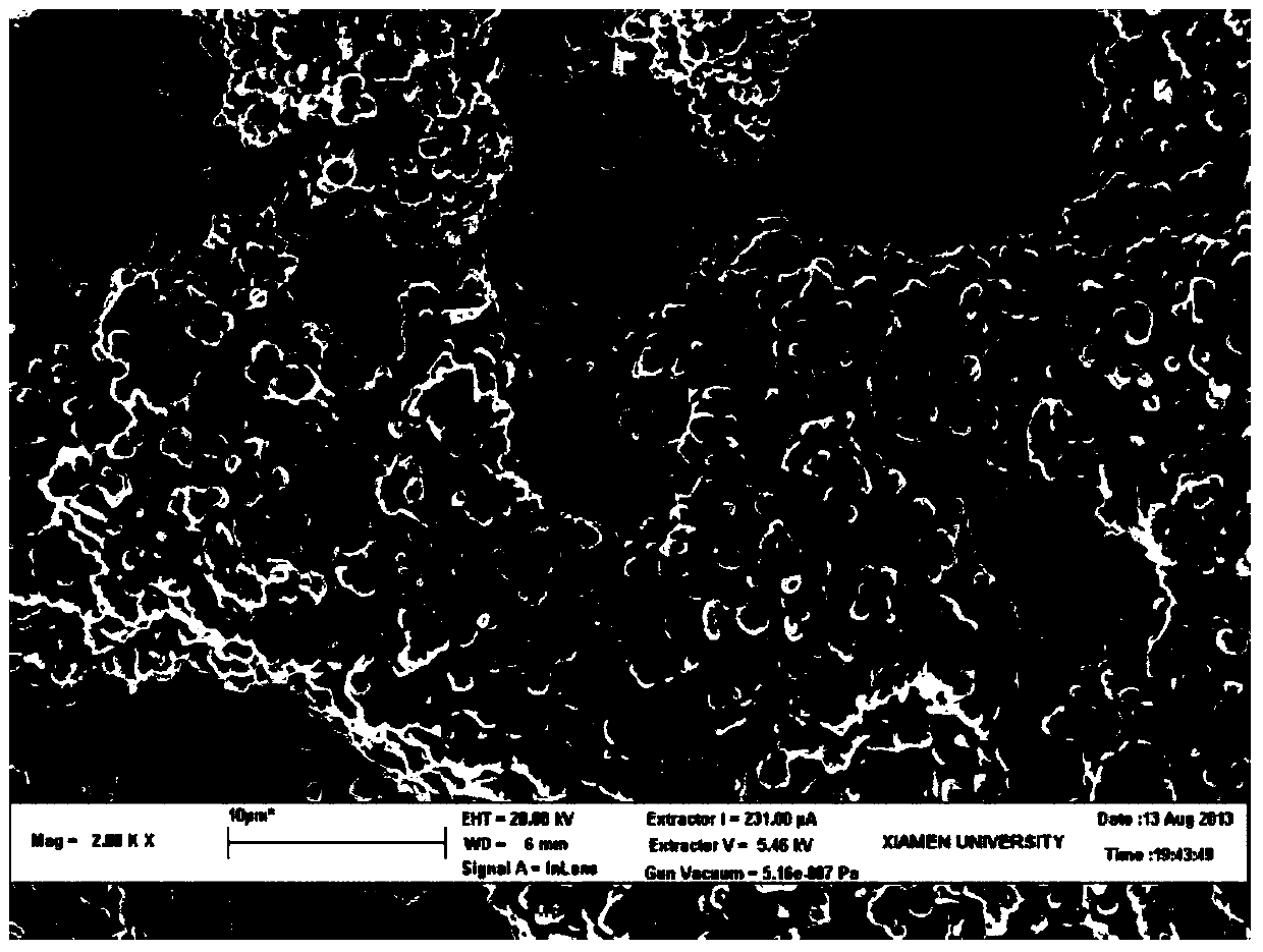
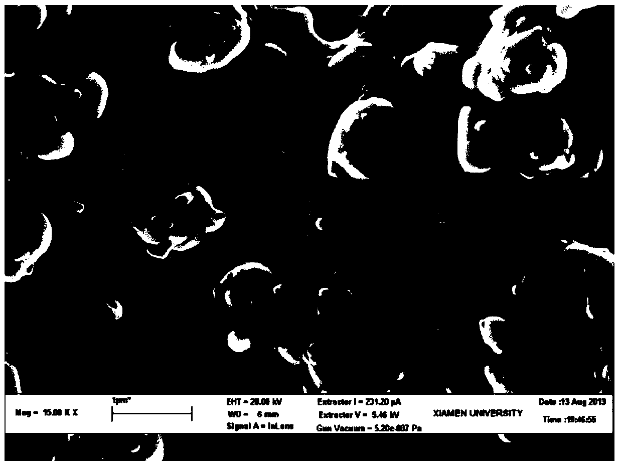
[0033] The molybdenum paste was screen printed or scraped on the ceramic substrate, dried at 200°C, then heat treated at 1100°C for 0.5 hours, and kept at 200°C for 2 hours to prepare a conductive molybdenum film electrode (ie, the back electrode). By using a scanning electron microscope (SEM) to observe their surfaces and cross-sections (eg figure 1 and figure 2 Shown), using a four-probe resistance tester to measure the sheet resistance of the film for characterization, and calculate the resistivity. The American Society for Testing Materials (ASTM) sta...

Embodiment 2

[0038] Mix 7g molybdenum powder (particle size 0.01-50μm), 0.5g glass powder (lead-free glass powder), 0.5g terpineol, 1g polyethylene glycol-200, 0.25g polyethylene glycol-400, 0.1g epoxy Resin E44 (or E51), 0.005g NaOH, 0.1g ethyl cellulose, 0.01g dibutyl phthalate, 0.03g Span 85 (sorbitan trioleate), 0.5g ethanol, 0.005g silicone oil Put them together and mix evenly to prepare a composite conductive molybdenum paste.

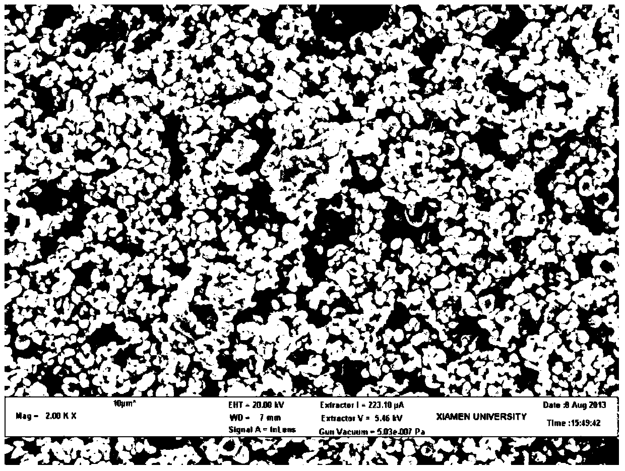
[0039] Molybdenum paste was screen-printed or scraped-coated on a ceramic substrate, dried at 200°C, then heat-treated at 900°C for 0.5 hours, and kept at 200°C for 2 hours to prepare a conductive molybdenum film electrode. By using a scanning electron microscope (SEM) to observe their surfaces and cross-sections (eg image 3 and Figure 4Shown), using a four-probe resistance tester to measure the sheet resistance of the film for characterization, and calculate the resistivity. The American Society for Testing Materials (ASTM) standard test method ASTM-D33...


PUM

PropertyMeasurementUnit
particle diameteraaaaaaaaaa
boiling pointaaaaaaaaaa

Abstract

The invention discloses a method for manufacturing copper indium gallium diselenide thin-film solar cells. The method comprises the steps that (1), compound conductive molybdenum thick liquid is arranged on a ceramic substrate in a silk-screen printing or blade coating or spraying mode, and back electrodes are obtained after drying of 150-250 DEG C, heat processing of 450-1150 DEG C and annealing of 150-250 DEG C, wherein the compound conductive molybdenum thick liquid comprises the following components, by weight, 50-80 parts of molybdenum powder, 5-15 parts of glass powder, 10-25 parts of organic carriers and 5-10 parts of annexing agents; the organic carriers comprise epoxy resin and organic solvent, and the mass ratio between the epoxy resin and the organic solvent is (1-5):(9-20); the annexing agents comprise moderate NaOH, thickening agents, plasticizer and surface active agents; (2), the copper indium gallium diselenide thin-film solar cells are processed based on the back electrodes. Compared with the prior art, the compound conductive molybdenum thick liquid adopted in the method can process the back electrodes of the copper indium gallium diselenide thin-film solar cells through a non-vacuum processing technology, namely, the silk-screen printing method or the spraying method or the blade coating method, the process is simple and the manufacturing cost is lowered.

Description

technical field [0001] The invention belongs to the field of preparation of solar cell electrodes, and in particular relates to a method for preparing copper indium gallium selenium thin film solar cells. Background technique [0002] In today's increasingly serious energy crisis, the research and application of new energy is becoming increasingly important. As an important part of the new energy industry, solar energy has the advantages of being clean, pollution-free, inexhaustible, safe and harmless. CIGS solar cells have the characteristics of stable performance, strong radiation resistance, low production cost, environmental protection and high efficiency, and may become the next generation of commercialized thin-film solar cells. However, the solar energy industry still has disadvantages such as high cost and instability. In my country, the application of solar energy is basically still in large-scale power stations, and large-scale power stations are basically distrib...

Claims


Application Information

Patent Timeline
Patent Type & Authority Applications(China)
IPC IPC(8): H01B1/22H01B1/16H01B13/00H01L31/18H01L31/0224
CPCY02P70/50
Inventor 张风燕张然于洋云大钦李超
Owner XIAMEN UNIV
Why Eureka
Try Eureka