Light-emitting diode (LED) epitaxial wafer, manufacturing method of LED epitaxial wafer and LED chip including LED epitaxial wafer

A technology for LED epitaxial wafers and LED chips, which is applied in electrical components, circuits, semiconductor devices, etc., can solve the problems of many lattice defects and poor crystal quality of the active layer, and achieves improved luminous efficiency, crystal quality, and concentration. Effect

Active Publication Date: 2013-12-25
XIANGNENG HUALEI OPTOELECTRONICS
View PDF7 Cites 14 Cited by
  • Summary
  • Abstract
  • Description
  • Claims
  • Application Information

AI Technical Summary

Problems solved by technology

[0006] The present invention aims to provide an LED epitaxial wafer, its manufacturing method and an LED chip including the same, so as to solve the technical problems of poor crystallization quality of the active layer and many lattice defects existing in the existing LED devices

Method used


Image

  • Light-emitting diode (LED) epitaxial wafer, manufacturing method of LED epitaxial wafer and LED chip including LED epitaxial wafer
  • Light-emitting diode (LED) epitaxial wafer, manufacturing method of LED epitaxial wafer and LED chip including LED epitaxial wafer
  • Light-emitting diode (LED) epitaxial wafer, manufacturing method of LED epitaxial wafer and LED chip including LED epitaxial wafer

Examples


Embodiment 1

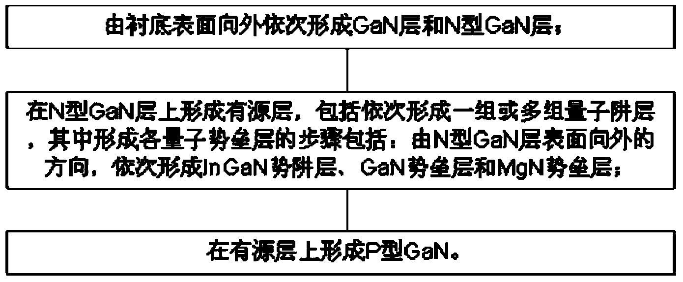
[0055] This embodiment provides a method for manufacturing an LED epitaxial wafer, comprising the following steps:

[0056] First, a GaN buffer layer, GaN layer, N-type AlGaN, and Si-doped N-type GaN are sequentially formed from the surface of the substrate outward, including the following steps:

[0057] Raise the temperature from room temperature to 1100°C, and process the substrate for 10 minutes under a hydrogen atmosphere with a pressure of 500mbar in the reaction chamber;

[0058] The temperature was lowered to 580°C, and the substrate was nitrided in a mixed atmosphere of hydrogen and nitrogen at a pressure of 500 torr in the reaction chamber. The treatment time was 5 minutes, and the volume fraction of hydrogen in the mixed atmosphere was 10%; Ethylgallium or trimethylgallium, a GaN buffer layer with a thickness of 540nm is grown on the substrate;

[0059] Raise the temperature to 1200°C, and in a mixed atmosphere of hydrogen and nitrogen at a pressure of 200torr, pas...

Embodiment 2

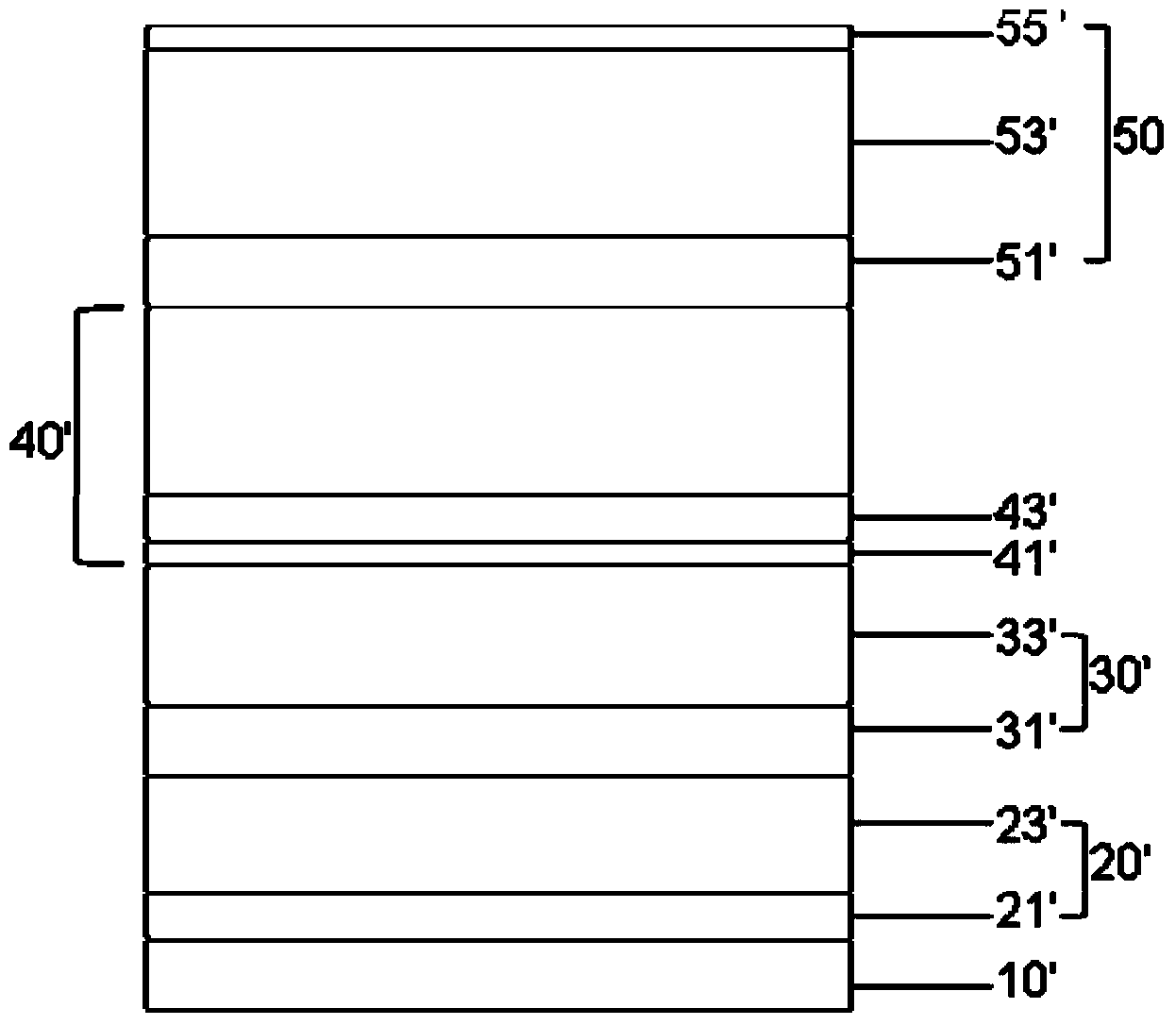
[0071] This embodiment provides a method for manufacturing an LED epitaxial wafer, wherein the steps of sequentially forming a GaN buffer layer 21, a GaN layer 23, an N-type AlGaN, and a Si-doped N-type GaN from the surface of the substrate outward, and The steps of forming a P-type AlGaN layer, a Mg-doped P-type GaN layer and a P-type GaN contact layer on the layer are the same as those in Embodiment 1.

[0072] In this embodiment, the step of forming the active layer on the N-type GaN layer: sequentially forming 10 groups of quantum well layers, forming each group of quantum well layers includes the following steps:

[0073] In a nitrogen atmosphere with a temperature of 730°C and a pressure of 300torr, trimethylgallium is introduced, and trimethylindium is grown to a thickness of 2.5nm, and the doping concentration of In is 3E+20atom / cm 3 InGaN potential well layer;

[0074] Stop feeding trimethyl indium, raise the temperature to 840°C, keep the pressure constant, and grow...

Embodiment 3

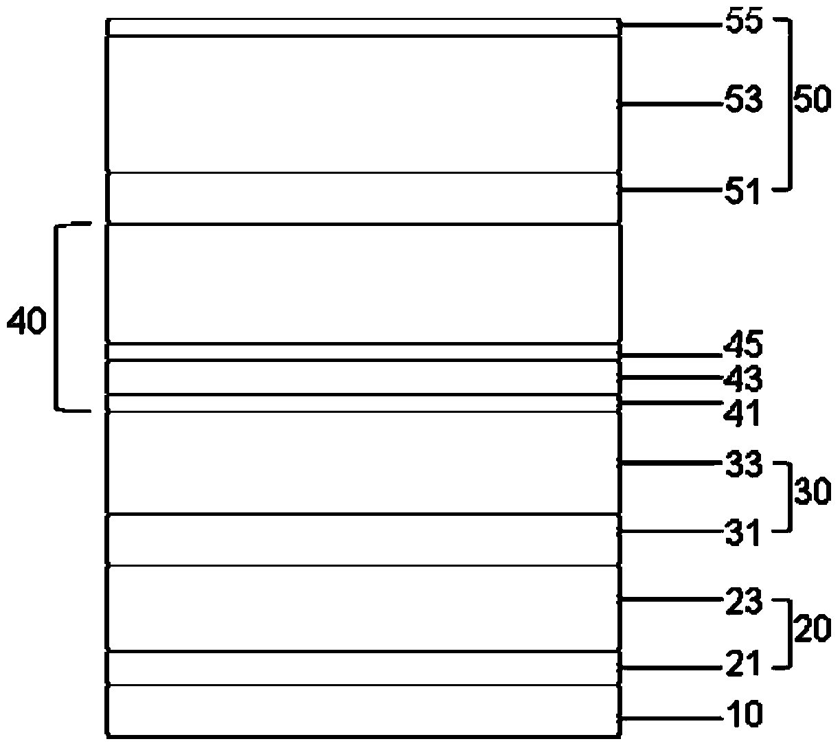
[0076] This embodiment provides a method for manufacturing an LED epitaxial wafer, wherein the steps of sequentially forming a GaN buffer layer, a GaN layer, N-type AlGaN, and Si-doped N-type GaN from the surface of the substrate outward, and on the active layer The steps of forming the P-type AlGaN layer, the Mg-doped P-type GaN layer and the P-type GaN contact layer are the same as those in Embodiment 1.

[0077] In this embodiment, the step of forming the active layer on the N-type GaN layer: sequentially forming 13 groups of quantum well layers, forming each group of quantum well layers includes the following steps:

[0078] In a mixed atmosphere of hydrogen and nitrogen at a temperature of 760°C and a pressure of 150 torr, triethylgallium and trimethylindium are injected to grow to a thickness of 3.5nm, and the doping concentration of In is 5E+20atom / cm 3 InGaN potential well layer, wherein the volume fraction of hydrogen in the mixed atmosphere is 15%;

[0079] Stop fee...


PUM


Abstract

The invention discloses a light-emitting diode (LED) epitaxial wafer, a manufacturing method of the LED epitaxial wafer and an LED chip including the LED epitaxial wafer. The LED epitaxial wafer comprises an undoped GaN layer, an N-type GaN layer, an active layer and a P-type GaN layer which are sequentially arranged from the substrate surface to the outside. The active layer comprises one or more groups of quantum well layers, wherein each quantum well layer comprises an InGaN potential well layer, a GaN potential barrier layer and an MgN potential barrier layer which are sequentially arranged in the direction away from a substrate. The manufacturing method of the LED epitaxial wafer comprises the steps of sequentially forming the undoped GaN layer, the N-type GaN layer, the active layer and the P-type GaN layer from the substrate surface to the outside, wherein the active layer forming step is that one or more groups of quantum well layers are sequentially formed, and the quantum well layer forming step is that the InGaN potential well layer, the GaN potential barrier layer and the MgN potential barrier layer are sequentially formed from the surface of the N-type GaN layer to the outside. By the adoption of the manufacturing method of the LED epitaxial wafer, the LED luminance and the internal quantum efficiency are improved.

Description

technical field [0001] The invention relates to the technical field of semiconductor lighting, in particular to an LED epitaxial wafer, a manufacturing method thereof and an LED chip comprising the same. Background technique [0002] GaN-based materials (including GaN, AlGaN, InGaN, MgGaN, and SiGaN) are direct bandgap semiconductors, and their bandgap is continuously adjustable from 1.8 to 6.2V. They are the most commonly used materials for producing high-brightness blue, green, and white LEDs. It is widely used in fields such as backlight, large-size screen display, signage indication, signal lamp and lighting. [0003] The manufacturing method of GaN-based LED chips is usually: use MOCVD (metal organic compound vapor deposition) to epitaxially grow a layer of GaN buffer layer on the substrate; then grow non-doped GaN, the purpose is to improve the quality of subsequent epitaxial crystals. On this basis, N-type GaN, active layer and P-type GaN are grown sequentially to fo...

Claims


Application Information

Patent Timeline
Patent Type & Authority Applications(China)
IPC IPC(8): H01L33/06H01L33/00
Inventor 王霄季辉徐迪梁智勇
Owner XIANGNENG HUALEI OPTOELECTRONICS
Why Eureka
Try Eureka