Serially connected optical switch based photon delay structure and numerical-control integrated photon delay device

A technology of delay device and integrated photonics, applied in the direction of optical waveguide light guide, optical waveguide coupling, etc., can solve the problems of inability to achieve large delay tuning, limited operating bandwidth, large energy consumption, etc., to achieve fast delay switching capability, RF broadband transparency , the effect of fast tuning

Inactive Publication Date: 2014-01-22
THE 44TH INST OF CHINA ELECTRONICS TECH GROUP CORP
View PDF3 Cites 13 Cited by
  • Summary
  • Abstract
  • Description
  • Claims
  • Application Information

AI Technical Summary

Problems solved by technology

[0004] At present, materials such as atomic vapor, optical fiber, and crystal are mainly used in the existing technology, and tunable optical retarders are realized through slow light effects such as electromagnetically induced transparency, four-wave mixing, stimulated Brillouin scattering, and optical resonance energy storage. However, due to the inherent defects of one kind or another in these technologies, it is difficult to meet the increasingly high performance requirements of the engineering community for the adjustable optical retarder;
[0005] It is difficult to obtain a small-volume device for both the atomic steam realization method and the crystal material realization method, which not only makes the cost high, but more importantly, greatly restricts its application range; the atomic steam realization method requires high temperature and high pressure conditions to produce delay effects , the energy consumption is huge. Although the implementation of atomic steam can achieve a wide range of optical delay, the dispersion and slow light effect it uses seriously limits its working bandwidth (the bandwidth value is generally in the order of MHz), which cannot meet the current GHz order. The communication bandwidth is required, and the delay tuning of the atomic vapor implementation is extremely difficult, and the adjustment flexibility is very poor; the conventional optical fiber delay implementation needs to cooperate with the optical switch to complete the delay tuning, but the length of the optical fiber is affected by the processing accuracy, ambient temperature and stress. , it is difficult to make breakthroughs in high precision and stability, which is also one of the important factors restricting the development of optically controlled phased arrays
[0006] In order to solve the above problems, those skilled in the art have also carried out unremitting explorations, and a silicon-based ultra-compact integrated photonic delay device has emerged during the exploration process (see Fengnian Xia, Lidija Sekaric and Yurii Vlasov, "Ultracompact optical buffers on a silicon chip", Nature Photonics, Vol.1, 2007, 65-71), the device is based on a nanometer-sized waveguide through a semiconductor process on an SOI silicon wafer, and cascades up to hundreds of microring resonant structures A delay device is formed to achieve a signal delay of 500 ps. Although this method has a large amount of delay, it cannot be tuned and does not meet the needs of dynamic tuning.
Since then, many delay devices based on microring resonant structures have appeared, such as Jaime Cardenas, etc., "Wide bandwidth continuously tunable optical delayline using silicon microring resonator", Oprics Express, Vol.18, No.25 and Qing Li, etc. , "Low loss microdisk-based delay line dor narrowband optical filters", Photonics Technology Letter, Vol.24, No.15, etc., all of which describe delay devices based on resonant structures such as microrings or microdisks. Although this delay device overcomes However, due to the constraints of the product constant of bandwidth and time, it is impossible to achieve large delay tuning under large bandwidth. At the same time, silicon-based delay devices basically use thermo-optic effect for delay tuning, and the tuning speed is in the range of On the order of hundreds of microseconds, it is also not suitable for high-speed applications

Method used


Image

  • Serially connected optical switch based photon delay structure and numerical-control integrated photon delay device
  • Serially connected optical switch based photon delay structure and numerical-control integrated photon delay device
  • Serially connected optical switch based photon delay structure and numerical-control integrated photon delay device

Examples


Embodiment Construction

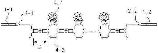
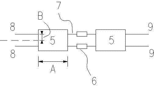
[0031] A digitally controlled integrated photon delay device based on a series optical switch, the digitally controlled integrated photon delay device is composed of two sections of coupling fibers, two mode-spot converters, a plurality of optical switches 3 and multiple sections of single-mode waveguides; the two sections of coupling fibers are respectively Recorded as input coupling fiber 1-1 and output coupling fiber 1-2; the mode spot converter is a waveguide shaped as an isosceles trapezoid, and the long base of the isosceles trapezoid forms the input end of the mode spot converter, and the isosceles trapezoid The narrow bottom edge of the optical switch 3 forms the output end of the speckle converter, and the two speckle converters are respectively recorded as the input speckle converter 2-1 and the output speckle converter 2-2; the optical switch 3 is an SOI-MMI optical switch, the optical switch 3 adopts a dual-input dual-output mode;

[0032] The output end of the inp...


PUM


Abstract

A serially connected optical switch based photon delay structure comprises a plurality of optical switches and multiple sections of single mode waveguides, wherein one input end of a first optical switch is connected with an input optical fiber, and the other input end of the first optical switch is idle; two output end of the first optical switch are connected with two input ends of a second optical switch respectively through two sections of single mode waveguides; other optical switches are sequentially connected in series according to the connection mode of the first optical switch and the second optical switch; one output end of an Nth optical switch is connected with an output optical fiber, and the other output end of the Nth optical switch is idle; and every two optical switches are connected through a first single mode waveguide and a second single mode waveguide, and the first single mode waveguide is longer than the second single mode waveguide. The serially connected optical switch based photon delay structure has the benefits as follows: the serially connected optical switch based photon delay structure has the advantages of high tuning speed, working stabilization and controllability and realizes mass production by virtue of a mature CMOS (complementary metal oxide semiconductor) technology; and besides, a numerical-control integrated photon delay device is integrated on an SOI (silicon on insulator) silicon chip, the size is small, and the integration level is high.

Description

technical field [0001] The invention relates to a technology capable of dynamically changing the optical transmission delay, in particular to an optical delay structure based on a series optical switch and a digitally controlled integrated photon delay device. Background technique [0002] Tunable photon delayer is a device used to dynamically change the delay of optical transmission. At present, this device is widely used in communication, quantum information processing and storage, radio astronomy and other fields to delay optical signals. Processing, and this device may also have important application prospects in future photonic computers. [0003] Different radio frequency signals and application fields have different delay range and accuracy requirements for tunable photonic delayers, but with the improvement of communication speed and working frequency band, the general development direction of tunable photonic delayers is to high precision , large-scale, fast ad...

Claims


Application Information

Patent Timeline
Patent Type & Authority Applications(China)
IPC IPC(8): G02B6/35G02B6/28G02B6/42G02B6/12
Inventor 瞿鹏飞孙力军
Owner THE 44TH INST OF CHINA ELECTRONICS TECH GROUP CORP
Why Eureka
Try Eureka