SiC Schottky diode and manufacturing method thereof

A technology of Schottky diodes and manufacturing methods, which is applied in semiconductor/solid-state device manufacturing, semiconductor devices, electrical components, etc., can solve the problems of SiC Schottky diodes without examples, achieve matching cost saving, simple manufacturing process, and reduce The effect of on-resistance

Active Publication Date: 2014-02-12
江苏中科汉韵半导体有限公司
View PDF4 Cites 9 Cited by
  • Summary
  • Abstract
  • Description
  • Claims
  • Application Information

AI Technical Summary

Problems solved by technology

[0006] In view of the above application needs, the present invention proposes a SiC Schottky diode with low conduction voltage and high reverse blocking voltage and its manufacturing method, which is currently applied to the SiC Schottky diode with this structure in the existing switching power supply and PFC circuit. Terki Diode has no examples yet

Method used


Image

  • SiC Schottky diode and manufacturing method thereof
  • SiC Schottky diode and manufacturing method thereof
  • SiC Schottky diode and manufacturing method thereof

Examples


Embodiment Construction

[0032] In order to make the object, technical solution and advantages of the present invention clearer, the present invention will be described in further detail below in conjunction with specific embodiments and with reference to the accompanying drawings.

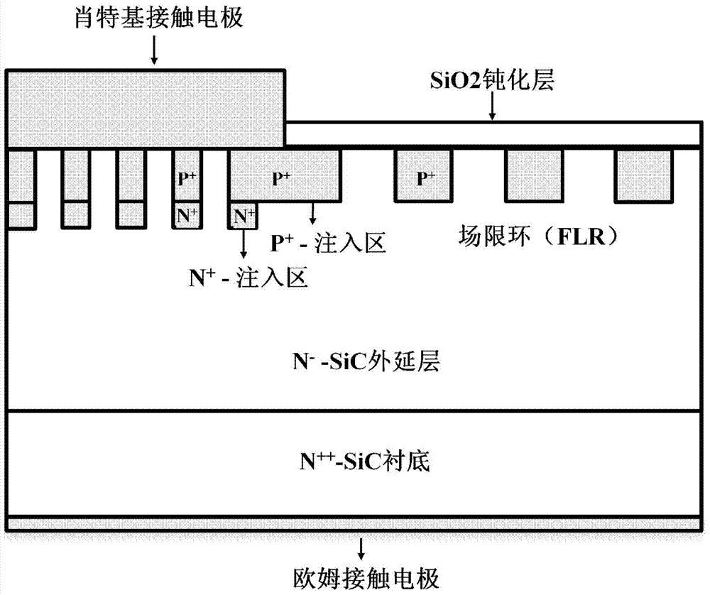
[0033] Such as figure 1 as shown, figure 1 The sectional view of the SiC Schottky diode with low turn-on voltage and high reverse blocking voltage provided for the present invention, the SiC Schottky diode includes N ++ -SiC substrate and N - - SiC epitaxial layer, N - - SiC epitaxial layer formed on N ++ -on SiC substrate, and N ++ -N-type ohmic contact electrodes are provided on the back of the SiC substrate, N - - There is a Schottky contact electrode on the surface of the SiC epitaxial layer, and there is a selective P under the Schottky contact electrode + -SiC domain ring, P + -SiC area under the ring with P + -N corresponding to SiC domain ring + - SiC area ring, as a protection ring during avalanche break...


PUM


Abstract

The invention discloses a SiC Schottky diode and a manufacturing method of the SiC Schottky diode. The SiC Schottky diode comprises an N++-SiC substrate and an N--SiC epitaxial layer, wherein the N--SiC epitaxial layer is formed on the N++-SiC substrate, an N-type ohmic contact electrode is arranged on the reverse side of the N++-SiC substrate, a Schottky contact electrode is arranged on the surface of the N--SiC epitaxial layer, a selective P+-SiC area ring is arranged at the bottom of the Schottky contact electrode, an N+-SiC area ring which corresponds to the P+-SiC area ring is arranged at the bottom of the P+-SiC area ring, and serves as a protective ring when avalanche breakdown is carried out, a plurality of P+-SiC protective rings are arranged at the periphery of the Schottky contact electrode, and serve as a terminal protective structure of a diode device, a SiO2 passivation layer is arranged on the edge of the Schottky contact electrode, and a field plate is arranged on the top of the SiO2 passivation layer. According to the SiC Schottky diode and the manufacturing method of the SiC Schottky diode, the break-over voltage of the SiC Schottky diode can be close to the break-over voltage of a Si Schottky diode, and the SiC Schottky diode is in good cooperation with an existing system with a Si device, and can be applied to a switching power source with the high voltage ranging from 600V to 1200V and a power factor correction circuit, wherein the high voltage cannot be achieved when the Si Schottky device is used.

Description

technical field [0001] The invention relates to the technical field of semiconductor devices, in particular to a SiC Schottky diode with low turn-on voltage and a manufacturing method thereof. Background technique [0002] Wide bandgap semiconductors generally refer to silicon carbide (SiC), gallium nitride (GaN), etc. with a bandgap width of about 3.0 eV or above. Compared with Si materials, these materials have the advantages of wider band gap, high breakdown electric field, high thermal conductivity, high electron saturation rate, etc., and are the preferred materials for preparing power electronic devices. Among them, the Schottky diode made of SiC material is a majority carrier device. This structure is characterized by no injection and storage of additional carriers, fast switching speed, and low switching loss. It can be widely used in electric vehicles / hybrids Inverters, converters, PFC circuits that require power conversion such as vehicles, as well as rectificatio...

Claims


Application Information

Patent Timeline
Patent Type & Authority Applications(China)
IPC IPC(8): H01L29/872H01L29/06H01L29/47H01L21/329
CPCH01L29/24H01L29/36H01L29/66143H01L29/872
Inventor 刘新宇许恒宇汤益丹蒋浩杰赵玉印申华军白云杨谦
Owner 江苏中科汉韵半导体有限公司
Why Eureka
Try Eureka