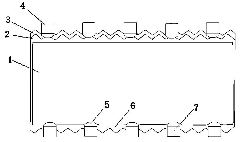
Preparation method of P-type crystal silicon double-sided cell
A double-sided battery and crystalline silicon technology, which is applied in semiconductor/solid-state device manufacturing, circuits, photovoltaic power generation, etc., can solve the problems of high production cost and restricted application range, so as to improve utilization rate, increase power generation, and avoid high temperature mixing The effect of the hashing and masking process
- Summary
- Abstract
- Description
- Claims
- Application Information
AI Technical Summary
Problems solved by technology
Method used
Image
Examples
Embodiment 1
[0028] A method for preparing a P-type crystalline silicon double-sided battery, the method comprising the following steps:
[0029] (a) P-type silicon substrate texturing:
[0030] Select a P-type silicon wafer with a resistivity of 0.3 ? Dilute about 5% hydrochloric acid and hydrofluoric acid for cleaning to remove surface impurities;
[0031] (b) Phosphorus is diffused on the front surface of the P-type silicon substrate to form a PN junction:
[0032] In a diffusion furnace at a temperature of 600°C, using POCl 3 Perform phosphorus diffusion to make the square resistance range 40-120? / □;
[0033] (c) Removal of phosphosilicate glass, back PN junction, and side PN junction:
[0034] In single-side etching equipment, use a mixed solution of 5% hydrofluoric acid and 50% nitric acid to etch the back surface and edge of the silicon wafer;
[0035] (d) Anti-reflection coating deposited on both sides:
[0036] On the front surface of the substrate, that is, on the side of t...
Embodiment 2
[0044] A method for preparing a P-type crystalline silicon double-sided battery, the method comprising the following steps:
[0045] (a) P-type silicon substrate texturing:
[0046] Select a P-type silicon wafer with a resistivity of 5??cm, and use 1.0% potassium hydroxide solution to chemically etch the surface of the P-type single crystal silicon at 80°C to prepare a pyramid-shaped light-trapping structure texture, and then use Dilute about 10% hydrochloric acid and hydrofluoric acid for cleaning to remove surface impurities;
[0047] (b) Phosphorus is diffused on the front surface of the P-type silicon substrate to form a PN junction:
[0048] In a diffusion furnace at a temperature of 800°C, using POCl 3 Perform phosphorus diffusion to make the square resistance range 40-120? / □;
[0049] (c) Removal of phosphosilicate glass, back PN junction, and side PN junction:
[0050] In single-side etching equipment, use a mixed solution of 10% hydrofluoric acid and 60% nitric acid...
Embodiment 3
[0060] A method for preparing a P-type crystalline silicon double-sided battery, the method comprising the following steps:
[0061] (a) P-type silicon substrate texturing:
[0062] Select a P-type silicon wafer with a resistivity of 10??cm, and use 2.0% sodium hydroxide solution to chemically etch the surface of the P-type single crystal silicon at 85°C to prepare a pyramid-shaped light-trapping structure texture, and then use Dilute about 10% hydrochloric acid and hydrofluoric acid for cleaning to remove surface impurities;
[0063] (b) Phosphorus is diffused on the front surface of the P-type silicon substrate to form a PN junction:
[0064] In a diffusion furnace at a temperature of 900°C, using POCl 3 Perform phosphorus diffusion to make the square resistance range 40-120? / □;
[0065] (c) Removal of phosphosilicate glass, back PN junction, and side PN junction:
[0066] In single-side etching equipment, use a mixed solution of 15% hydrofluoric acid and 70% nitric acid...
PUM
| Property | Measurement | Unit |
|---|---|---|
| Thickness | aaaaa | aaaaa |
| Thickness | aaaaa | aaaaa |
| Thickness | aaaaa | aaaaa |
Abstract
Description
Claims
Application Information
