Single-photon-level resolution ratio sensor unit structure based on standard CMOS technology

A sensor unit and single photon technology, applied in electrical components, semiconductor devices, circuits, etc., can solve the problems of time resolution not reaching photon counting, large unit structure volume, high operating voltage, etc., to achieve large-scale integration , Simple device structure and compatible manufacturing process

Inactive Publication Date: 2014-05-07
苏州超锐微电子有限公司
View PDF4 Cites 42 Cited by
  • Summary
  • Abstract
  • Description
  • Claims
  • Application Information

AI Technical Summary

Problems solved by technology

The photomultiplier tube (PMT) commonly used today requires high operating voltage, and the unit structure is bulky, which cannot be integrated on a large scale
Silicon avalanche photodiodes (APD) work in the linear region of the PN junction, and the working voltage is lower than the avalanche voltage, so its gain is generally not higher than 1000, and single photon detection cannot be realized
The gain of electron multiplier CCD (EM-CCD) can be applied to weak light detection, but its operating frequency is low, and the time resolution cannot reach the application of photon counting

Method used


Image

  • Single-photon-level resolution ratio sensor unit structure based on standard CMOS technology
  • Single-photon-level resolution ratio sensor unit structure based on standard CMOS technology
  • Single-photon-level resolution ratio sensor unit structure based on standard CMOS technology

Examples


Embodiment Construction

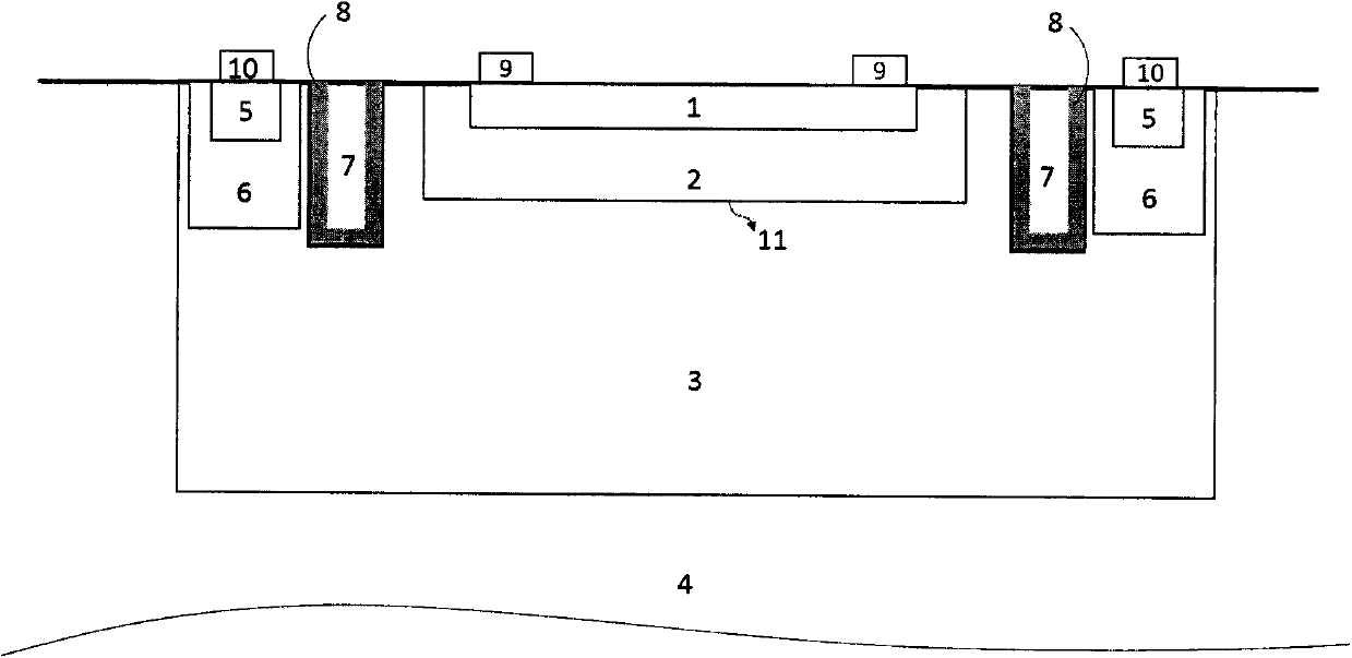
[0013] In the following detailed description, specific details are described in order to provide a comprehensive understanding of the invention. As previously stated, it will be understood that if the type of semiconductor doping is reversed (i.e., N-type doping replaces P-type doping), the voltage, Where the anode and cathode etc. are appropriately reversed, the examples given for P-type and N-type materials are used equally. The present invention assumes the use of a P-type substrate, which is the most standard substrate type used in standard CMOS processes.

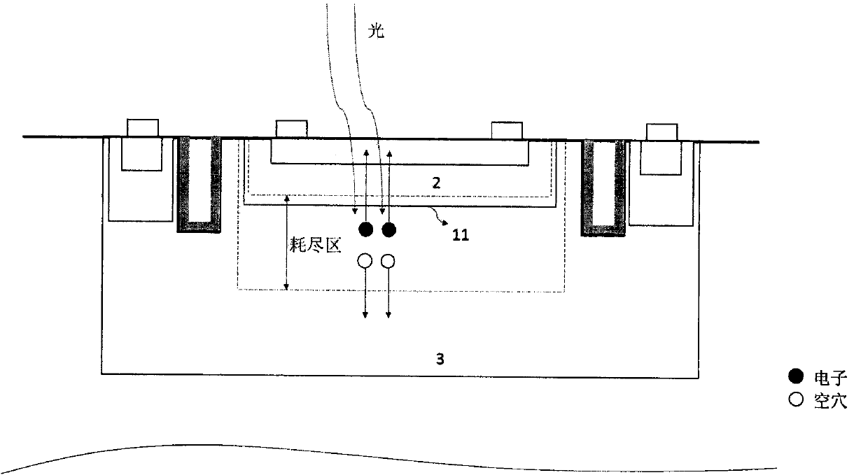
[0014] figure 1 It is a schematic diagram of the single-photon-level resolution sensor unit structure based on the standard CMOS process of the present invention. The composition of the single-photon-level resolution sensor unit structure is: a deep N well (3) is arranged above the P-type silicon substrate (4) ; P-well region (2) is formed above and surrounded by deep N-well (3); anode contact (9) is connected to P-we...


PUM


Abstract

Disclosed is a single-photon-level resolution ratio sensor unit structure based on the standard CMOS technology. The single-photon-level resolution ratio sensor unit structure uses an SPAD. According to the single-photon-level resolution ratio sensor unit structure, basically, a deep N-well (3) is arranged above a P-type silicon substrate (4), a P-well area (2) is formed above the deep N-well (3) and wrapped by the deep N-well (3), an anode contact (9) is connected to the P-well area (2) through a heavy-doping P-well area (1), a cathode contact (10) is connected to an N-well area (6) and the deep N-well (3) through a heavy-doping N-well area (5), a shallow trench isolation area (7) is located between the P-well area (2) and the N-well area (6) to isolate a P-well from an N-well, a P-type doped protection ring (8) surrounds the shallow trench isolation area (7) so as to restrain dark noise caused by defects in shallow trench isolation, and a PN junction (11) is arranged between the bottom of the P-well area (2) and the deep N-well (3); the PN junction generates a high-voltage area when proper bias voltage is applied between the cathode and the anode, and an SPAD multiplication area is formed so as to explore photons; the breakdown voltage of the edge of the PN junction is higher than that of the SPAD plane multiplication area by controlling the concentration gradient of the deep N-well (3).

Description

technical field [0001] The invention is a unit structure of a single-photon-level resolution sensor, and its manufacturing method is specifically implemented in a standard CMOS process. Background technique [0002] High-efficiency, low-noise single-photon detectors are needed in the fields of weak light imaging, high-speed imaging, and quantum communication. The commonly used photomultiplier tube (PMT) needs high operating voltage, and the unit structure is bulky, so it cannot be integrated on a large scale. A silicon avalanche photodiode (APD) works in the linear region of the PN junction, and its working voltage is lower than the avalanche voltage, so its gain is generally not higher than 1000, and single photon detection cannot be realized. The gain of electron multiplier CCD (EM-CCD) can be applied to weak light detection, but its operating frequency is low, and the time resolution cannot reach the application of photon counting. [0003] Single-photon avalanche diode...

Claims


Application Information

Patent Timeline
Patent Type & Authority Applications(China)
IPC IPC(8): H01L31/107H01L31/0352
CPCH01L31/107H01L31/035272
Inventor 卜晓峰朱小茅吴俊辉
Owner 苏州超锐微电子有限公司
Why Eureka
Try Eureka