High-resistance temperature coefficient vanadium oxide film preparation method

A technology of vanadium oxide thin film and temperature coefficient, applied in ion implantation plating, metal material coating process, coating, etc., can solve the problem of increasing vanadium oxide thin film, increasing the complexity and difficulty of reactive sputtering process, and intrinsic noise of thin film Increase and other issues to achieve good compatibility

Active Publication Date: 2014-06-25
WUXI ALEADER INTELLIGENT TECH
View PDF2 Cites 11 Cited by
  • Summary
  • Abstract
  • Description
  • Claims
  • Application Information

AI Technical Summary

Problems solved by technology

However, the doping of transition metal elements not only increases the complexity and difficulty of reactive sputtering process control, but also may increase the non-uniformity of the microstructure in the vanadium oxide film due to doping, resulting in an increase in the intrinsic noise of the film.

Method used


Image

  • High-resistance temperature coefficient vanadium oxide film preparation method
  • High-resistance temperature coefficient vanadium oxide film preparation method
  • High-resistance temperature coefficient vanadium oxide film preparation method

Examples


preparation example Construction

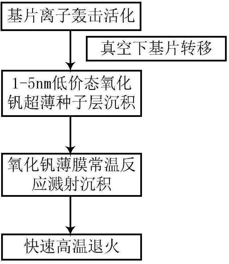
[0022] The preparation method provided by the present invention is suitable for preparing vanadium oxide thermosensitive films with high resistance temperature coefficient, and the preparation process is as follows:

[0023] (1) Activate the surface of the substrate in an oxygen-rich atmosphere, and then transfer the processed substrate to the sputtering chamber.

[0024] (2) Two-step sputtering deposition: at room temperature, first sputter with low oxygen or even oxygen free, deposit a seed layer of 1-5nm thick with high nucleation density on the surface of the substrate, and then sputter the vanadium oxide film with normal reaction Deposition.

[0025] (3) Rapid annealing treatment: in the same atmosphere as reactive sputtering, at a predetermined temperature of 300~500℃, using annealing equipment such as infrared rapid annealing furnace, the sputtered vanadium oxide film is subjected to a short time high temperature for 2-10 minutes Heat treatment.

Embodiment 1

[0028] This example is used to evaluate the temperature coefficient of resistance of the vanadium oxide thin film prepared on the silicon wafer deposited with the silicon nitride thin film by the method of the present invention. details as follows:

[0029] Deposit ~100nm thick Si on silicon wafer using CVD process 3 N 4 The thin film is cleaned and dried by a standard semiconductor cleaning process and used as the substrate for the deposition of the vanadium oxide thin film; before sputtering, the vacuum degree of the vacuum chamber where the Kaufman source is located is pumped to better than 5.0×10 -4 After Pa, open the intake valve and pass in O 2 / Ar flow ratio 1:6 ultra-high purity Ar and O 2 , And maintain the vacuum at ~3.0×10 -1 Pa, and then ion bombard the surface of the substrate for 3 minutes. The activated substrate is transferred to the sputtering chamber under the vacuum environment, and the two-step sputtering deposition at room temperature is carried out: 2 / Ar flo...

Embodiment 2

[0037] Through this example to evaluate the method of the present invention in depositing SiO 2 The temperature coefficient of resistance of the vanadium oxide thin film prepared on the thin silicon wafer. details as follows:

[0038] Deposit ~100nm thick SiO on silicon wafer using CVD process 2 The thin film is cleaned and dried by a standard semiconductor cleaning process and used as the substrate for the deposition of the vanadium oxide thin film; before sputtering, the vacuum degree of the vacuum chamber where the Kaufman source is located is pumped to be better than 5.0×10 -4 After Pa, open the intake valve and pass in O 2 / Ar flow ratio 1:15 ultra-high purity Ar and O 2 , And maintain the vacuum at ~5.0×10 -1 Pa, then ion bombard the surface of the substrate for 5 minutes. The activated substrate is transferred to the sputtering chamber under the vacuum environment, and the two-step sputtering deposition at room temperature is carried out: 2 / Ar flow ratio is 1:45 to deposit...


PUM


Abstract

The invention discloses a high-resistance temperature coefficient vanadium oxide film preparation method which comprises the following steps: (1) performing ion bombardment activation treatment on a substrate in an oxygen-enriched atmosphere; (2) performing vanadium oxide film deposition in two steps at normal temperature: depositing a 1-5nm low-valence ultrathin vanadium oxide seed layer on the treated substrate, and then depositing a vanadium oxide film through reactive sputtering; and (3) rapidly annealing the film at a high temperature in the same atmosphere as reactive sputtering. By adopting the preparation method disclosed by the invention, vanadium oxide film deposition with the resistance temperature coefficient of -3-5% / K is achieved, and meanwhile the preparation method disclosed by the invention has good compatibility with a micro-electromechanical systems (MEMS) process and an integrated circuit manufacturing process, and is applicable to large-scale manufacturing of devices based on the vanadium oxide thermosensitive film.

Description

Technical field [0001] The invention relates to the technical field of detectors and sensors, in particular to a method for preparing high-resistance temperature coefficient vanadium oxide films, which can be used for the preparation of sensitive film materials based on thermal principles such as uncooled infrared detectors, terahertz detectors and sensors. Background technique [0002] Because of its advantages: (a) low noise, (b) high temperature coefficient of resistance, (c) good MEMS process compatibility, and (d) integrated circuit process compatibility, vanadium oxide film is widely used as a thermal film. Microbolometer type uncooled focal plane array with excellent detection performance and corresponding uncooled infrared detectors. [0003] With the development of terahertz science and technology, terahertz detection technology has shown broad application prospects in security inspection, short-range radar, medical imaging and other fields. The focal plane array detector...

Claims


Application Information

Patent Timeline
Patent Type & Authority Applications(China)
IPC IPC(8): C23C14/34C23C14/08C23C14/58
Inventor 韦良忠朱汪龙刘燕陈黎明
Owner WUXI ALEADER INTELLIGENT TECH
Why Eureka
Try Eureka