Organic electroluminescent device and preparing method thereof

An electroluminescent device and electroluminescent technology, which are applied in the directions of organic semiconductor devices, materials of organic semiconductor devices, and electric solid devices, etc., can solve the problems of failure, penetration, and poor water vapor and oxygen barrier properties of organic electroluminescent devices.

Active Publication Date: 2014-07-02
OCEANS KING LIGHTING SCI&TECH CO LTD +2
View PDF9 Cites 0 Cited by
  • Summary
  • Abstract
  • Description
  • Claims
  • Application Information

AI Technical Summary

Problems solved by technology

[0004] Flexible organic electroluminescent devices are the development trend of organic electroluminescent devices. Traditional flexible organic electroluminescent devices use metal materials as the cathode layer. Because metals are prone to pinholes and defects during evaporation preparation, this leads to water vapor Oxygen and oxygen easily penetrate into the organic electroluminescent device from pinholes and defects, resulting in the failure of the organic electroluminescent device, so the quality of the packaging directly affects the life of the organic electroluminescent device
[0005] Traditional organic electroluminescent devices have poor barrier properties to water vapor and oxygen, and their service life is not long

Method used


Image

  • Organic electroluminescent device and preparing method thereof
  • Organic electroluminescent device and preparing method thereof
  • Organic electroluminescent device and preparing method thereof

Examples


preparation example Construction

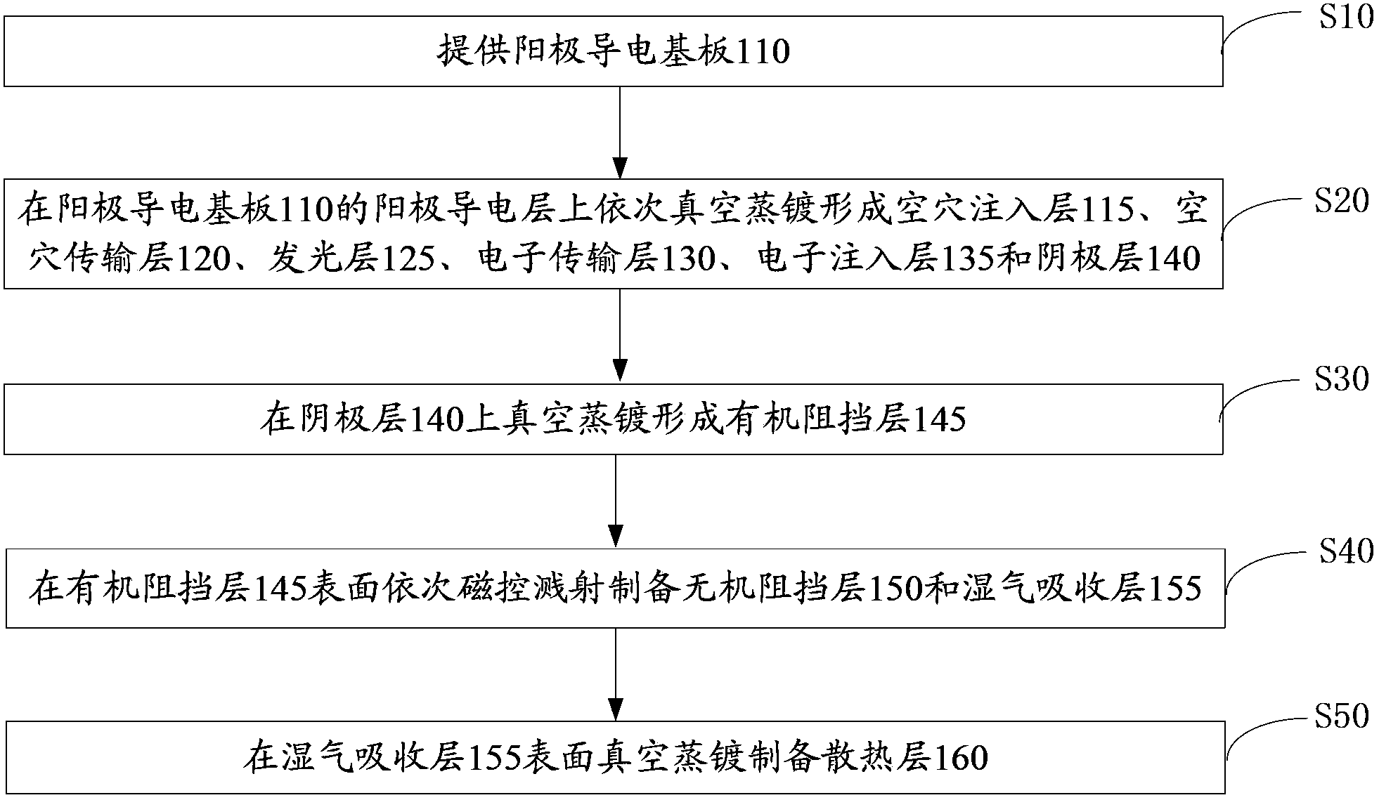
[0062] Such as figure 2 As shown, the preparation method of the above-mentioned organic electroluminescent device comprises the following steps:

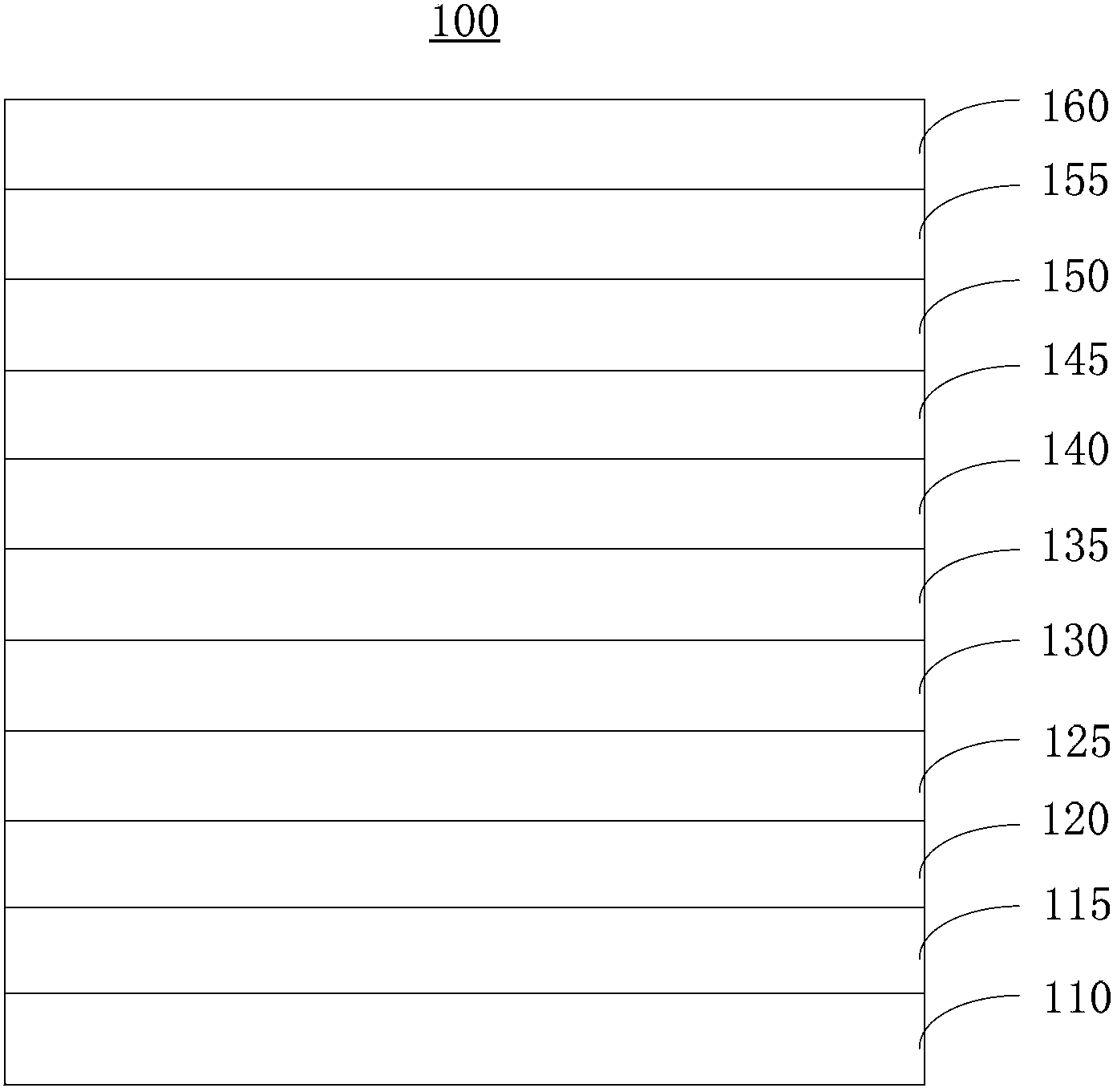
[0063] S10 , providing an anode conductive substrate 110 .

[0064] Including the anode conductive layer and the substrate, the substrate can be a glass substrate or an organic film substrate, and the material of the anode conductive layer can be a conductive oxide, such as indium tin oxide (ITO), aluminum-doped zinc oxide (AZO), indium-doped zinc oxide (IZO) or fluorine-doped tin oxide (FTO), these conductive oxides are prepared on glass substrates, referred to as ITO glass, AZO glass, IZO glass, FTO glass. The anode conductive substrate can be self-made or purchased from the market. In practical applications, other suitable materials can be selected as the anode conductive substrate 110 as required. In practical applications, desired anode patterns of organic electroluminescent devices can be prepared on the anode conductive s...

Embodiment 1

[0100] Provide an ITO glass substrate with a thickness of 100nm as a conductive substrate, and process it as follows: cleaning with acetone→cleaning with ethanol→cleaning with deionized water→cleaning with ethanol, all cleaning with an ultrasonic cleaner, each cleaning time is 5 minutes, and then Blow dry with nitrogen, and dry in an oven for later use. Surface activation treatment is also required for the cleaned ITO glass to increase the oxygen content on the surface of the conductive layer and improve the work function of the surface of the conductive layer.

[0101] In a vacuum of 3×10 -5 Under the condition of Pa, with Evaporation speed, vacuum evaporation method is used to form a hole injection layer on the ITO substrate; the material of the hole injection layer is doped with MoO 3 NPB, where MoO 3 The weight percentage of the hole transport layer is 30%, and the thickness of the formed hole transport layer is 10nm.

[0102] In a vacuum of 3×10 -5 Under the conditi...

Embodiment 2

[0112] The preparation method of the organic electroluminescence device of embodiment 2 is basically the same as embodiment 1, the difference is:

[0113] The desired anode pattern of the organic electroluminescent device is prepared on the surface-activated ITO glass.

[0114] In a vacuum of 5 x 10 -5 Under the condition of Pa, with The evaporation rate is high, and an organic barrier layer is formed on the cathode layer by vacuum evaporation. The material of the organic barrier layer is NPB, and the thickness of the formed organic barrier layer is 250 nm.

[0115] The background vacuum is 5×10 -4 Under the condition of Pa, an inorganic barrier layer is formed on the organic barrier layer by magnetron sputtering. The material of the inorganic barrier layer is Bi 2 Te and TaS 2 , where TaS 2 It accounts for 15% by weight of the inorganic barrier layer. The formed inorganic barrier layer had a thickness of 120 nm.

[0116] The background vacuum is 5×10 -4 Under the c...


PUM


Abstract

The invention discloses an organic electroluminescent device comprising an anode conductive substrate, a hole injection layer, a hole transporting layer, a light-emitting layer, an electron transporting layer, an electron injection layer, a cathode layer, an organic blocking layer, an inorganic blocking layer, a moisture absorption layer and a cooling layer which are stacked successively. According to the organic electroluminescent device, the material of the inorganic blocking layer adopts a mixture of telluride and sulfide, so advantages, such as high density, good water and oxygen prevention capability, etc., can be realized, and the material of the moisture absorption layer is selected from at least one calcium oxide, barium oxide, strontium oxide and magnesium oxide, so the water vapour in the air can be absorbed. Through the cooperation of the inorganic blocking layer and the moisture absorption layer, less water vapour and oxygen enter the organic electroluminescent device, and compared with a conventional organic electroluminescent device, the organic electroluminescent device has the advantage of long service life. The invention further discloses a preparing method of the organic electroluminescent device.

Description

technical field [0001] The invention relates to the field of electroluminescence, in particular to an organic electroluminescence device and a preparation method thereof. Background technique [0002] Organic Light Emitting Display (OLED) is a current-type semiconductor light-emitting device based on organic materials. Its typical structure is to make a layer of organic light-emitting material with a thickness of tens of nanometers on ITO glass as the light-emitting layer. There is a layer of metal electrodes with low work function on top of the layer. When a voltage is applied to the electrodes, the light-emitting layer produces light radiation. [0003] OLED devices have the advantages of active luminescence, high luminous efficiency, low power consumption, lightness, thinness, and no viewing angle restrictions. They are considered by industry insiders to be the new generation of devices that are most likely to occupy a dominant position in the future lighting and display...

Claims


Application Information

Patent Timeline
Patent Type & Authority Applications(China)
IPC IPC(8): H01L51/52H01L51/54H01L51/56
CPCH10K50/846H10K50/844H10K50/87H10K2102/00H10K71/00
Inventor 周明杰王平钟铁涛陈吉星
Owner OCEANS KING LIGHTING SCI&TECH CO LTD
Why Eureka
Try Eureka