Method for preparing photovoltaic material cuprous sulfide (Cu2S) film

A technology of cuprous sulfide and photovoltaic materials, applied in metal material coating process, ion implantation plating, coating, etc., can solve the problems of silicon solar cells, environmental pollution, high production cost, etc.

Inactive Publication Date: 2014-07-30
SHANGHAI UNIV
View PDF1 Cites 7 Cited by
  • Summary
  • Abstract
  • Description
  • Claims
  • Application Information

AI Technical Summary

Problems solved by technology

However, gallium arsenide is difficult to compete with silicon solar cells due to its complex production equipment, high energy consumption, and long production cycle, resulting in high production costs; among cadmium sulfide and cadmium telluride materials, cadmium is highly toxic and will cause serious damage to the environment. Pollution, although it has a high battery conversion efficiency, it is limited in application; for thin-film batteries made of copper indium selenium, indium and selenium are both scarce elements, expensive, and not suitable for large-scale production and application

Method used


Image

  • Method for preparing photovoltaic material cuprous sulfide (Cu2S) film
  • Method for preparing photovoltaic material cuprous sulfide (Cu2S) film

Examples


Embodiment 1

[0023] (1) Substrate cleaning: After cleaning the CdS / ITO substrate with Triton solution, rinse it with deionized water, then ultrasonically clean it in acetone, alcohol, and deionized water for 10 minutes, repeat the above ultrasonic cleaning process 3 times , rinse the substrate with deionized water, dry it with an argon gun, put it in a vacuum drying oven, and set it aside.

[0024] (2) Open the sputtering chamber and place Cu 2 S target material (purity greater than 99.999%), place the substrate in the corresponding position, cover the sputtering chamber, and turn on the mechanical pump to draw the vacuum to below 10 Pa. Then turn on the molecular pump and pump the background vacuum to 7×10 -4 Below Pa.

[0025] (3) Infuse argon gas (> 99.99%) to make the pressure of the sputtering chamber reach 0.5 Pa and keep it for 10 minutes.

[0026] (4) Adjust the power of the DC sputtering source to 90 W, ready for ignition. Pre-sputter for 10 min, clean the surface of the targ...

Embodiment 2

[0030] It is the same as the above-mentioned embodiment 1, except that the step 6 is that the substrate temperature is about 300 oC.

Embodiment 3

[0032] It is the same as the above-mentioned embodiment 1, except that the step 6 is different, and the substrate temperature is about 400 oC.

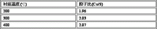
[0033] As shown in Table 1 below, Cu prepared under different substrate temperatures 2 The atomic weight ratio of the S thin film was maintained at Cu / S=2. Basically conforms to Cu 2 Atomic ratio of S.

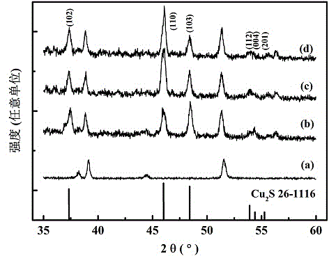
[0034] As shown in the attached picture figure 1 As shown, Cu prepared on CdS / ITO substrate 2 XRD image of S thin film and standard JCPDS card Cu 2 The peak position of S-1116 corresponds, which means that the prepared Cu 2 The S film is a chalcocite structure and belongs to the orthorhombic crystal system.

[0035]

[0036] Table 1 Cu deposition on CdS / ITO substrate at different substrate temperatures 2 Atomic ratio of S thin film (Cu / S)

[0037]


PUM

PropertyMeasurementUnit
thicknessaaaaaaaaaa

Abstract

The invention relates to a method for preparing a photovoltaic material cuprous sulfide (Cu2S) film, and discloses a technology for preparing the cuprous sulfide film in photovoltaic industry. The preparation method is based on a direct current magnetron sputtering technology. The method takes high purity cuprous sulfide as a sputtering target material and takes argon as a working gas, has characteristics of high deposition rate, controllable film thickness and good repeatability, can be used for preparing a large-area, uniform and high quality cuprous sulfide film, and is expected to realize industrial production of the cuprous sulfide film.

Description

technical field [0001] The invention relates to a method for preparing Cu by using DC magnetron sputtering technology 2 The method for S thin film belongs to the technical field of photoelectric thin film preparation. Background technique [0002] Energy is the driving force of social development, promoting the progress of human productivity and the continuous improvement of living standards. At present, in the world's energy structure, humans mainly use fossil energy, such as oil, coal, and natural gas. However, with the continuous growth of population and the rapid development of industry, traditional fossil energy is decreasing day by day. In addition, the environmental hazards caused by by-product emissions are becoming increasingly prominent. Fossil energy is bound to be replaced by new clean and renewable energy. Renewable energy has the characteristics of pollution-free and renewable, mainly including: solar energy, wind energy, water energy, geothermal energy, e...

Claims


Application Information

Patent Timeline
Patent Type & Authority Applications(China)
IPC IPC(8): C23C14/35C23C14/06
Inventor 王林军任兵沈心蔚黄健杨晓蓉杨惠敏唐可沈忠文夏义本
Owner SHANGHAI UNIV
Why Eureka
Try Eureka