A kind of preparation method of grating structure transparent conductive film
A technology of transparent conductive film and grating structure, applied to the conductive layer on the insulating carrier, ion implantation plating, coating, etc., which can solve the problems of long preparation time period, uneven product shape and size, low preparation efficiency, etc. , to achieve the effects of reducing environmental pollution and personal safety hazards, shortening sample preparation time, and improving light transmittance
- Summary
- Abstract
- Description
- Claims
- Application Information
AI Technical Summary
Problems solved by technology
Method used
Image

Examples
Embodiment 1
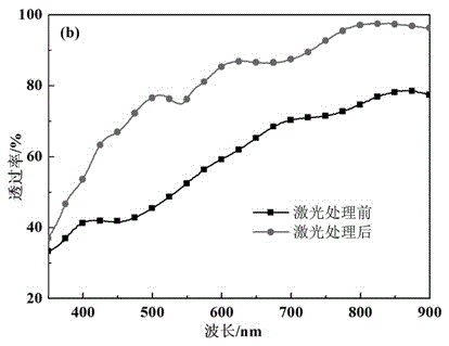
[0018] Preparation of Ag / FTO transparent conductive film: directly use commercially available FTO glass (thickness 750nm, average transmittance 80%, sheet resistance 8.5Ω / sq) as the substrate, use the method of cleaning the glass substrate, wash and dry, and then use high Vacuum DC magnetron sputtering apparatus sputters the Ag layer (the purity of the Ag target is 99.99%), the sputtering current is 60mA, the sputtering time is 3 seconds, the sputtering gas is argon, and metal Ag is deposited on the FTO glass substrate film , to obtain Ag / FTO transparent conductive film for future use.
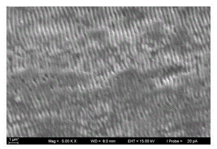
[0019] The Ag / FTO transparent conductive film grating structure is to scan the Ag / FTO transparent conductive film with a nanosecond laser with a pulse width of 1~2ns, a wavelength of 532nm, and a repetition rate of 1kHz. The method is as follows: adjust the position of the sample stage so that the surface of the Ag / FTO transparent conductive film is located at 2.5mm behind the laser focus; con...
Embodiment 2
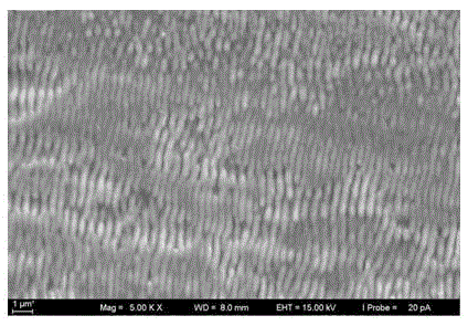
[0021] Preparation of Pt / FTO transparent conductive film: directly use commercially available FTO glass (thickness about 750nm, average transmittance 80%, sheet resistance 8.5Ω / sq) as the substrate, use the method of cleaning the glass substrate, after cleaning and drying, use The Pt layer was sputtered by a high-vacuum DC magnetron sputtering apparatus (the purity of the Pt target was 99.99%), the sputtering current was 60 mA, the sputtering time was 4 seconds, and the sputtering gas was argon. Deposit the metal Pt layer on the FTO glass base film.
[0022] The Pt / FTO transparent conductive film grating structure is to scan the Pt / FTO transparent conductive film with a nanosecond laser with a pulse width of 1~2ns, a wavelength of 532nm, and a repetition rate of 1KHz. The method is as follows: adjust the position of the sample stage so that the surface of the Pt / FTO transparent conductive film is located 2.5mm behind the laser focus; control the laser energy density to 1.0J / cm...
PUM
| Property | Measurement | Unit |
|---|---|---|
| thickness | aaaaa | aaaaa |
Abstract
Description
Claims
Application Information
PatSnap Eureka turns technology decisions into work you can execute. Powered by our Innovation Knowledge Graph, it runs expert workflows across engineering, life sciences, materials and intellectual property. Get your review-ready output in minutes.


