

Multi-quantum well solar cell and method of manufacturing multi-quantum well solar cell
A technology of solar cells and multiple quantum wells, applied in the field of solar cells, can solve problems such as inability to solve light conversion efficiency, and achieve the effects of high photoelectric conversion efficiency and low cost
- Summary
- Abstract
- Description
- Claims
- Application Information
AI Technical Summary
Problems solved by technology
Method used
Image

Examples
Embodiment 1
[0095]
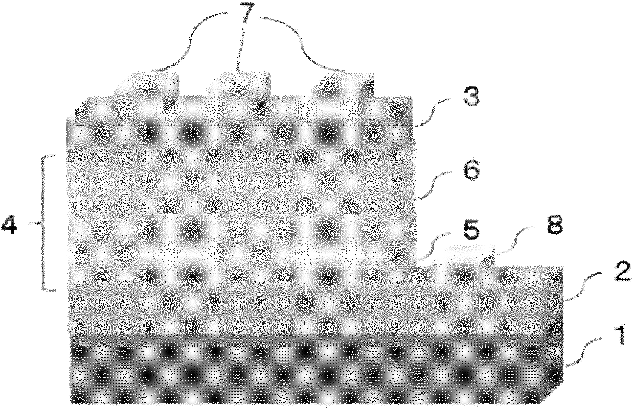
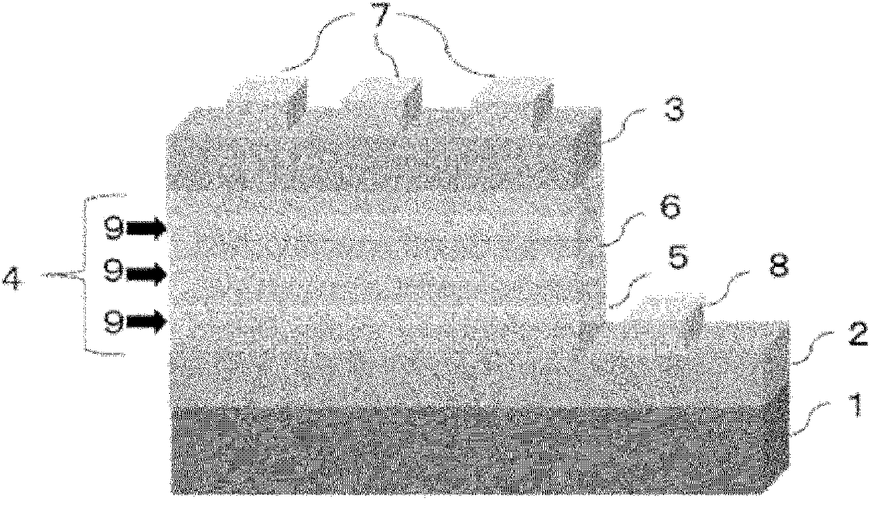
[0096] On a sapphire substrate 1 having a thickness of 450 μm, a ZnO buffer film was formed by a nitrogen addition crystallization method. The sputtering method was used for film formation, and the gas flow rate was adjusted so that the pressure might become 0.3 Pa in a sputtering apparatus, and argon gas and nitrogen gas were introduced. The flow rate of argon and nitrogen is set to [N 2 ] = 2 sccm, [Ar] = 20 sccm. By introducing nitrogen into the sputtering device, nitrogen molecules dissociate in the device to generate nitrogen atoms, thereby forming a ZnO film on the substrate. The substrate temperature was set to 700°C.
[0097] Next, GaN having a lattice constant of 0.319 nm was stacked by MOCVD to form p-type semiconductor layer 2 . Magnesium is used in the p-type dopant. Set the substrate temperature to 1150°C, pour trimethylgallium as the Ga raw material, pour ammonia water as the N raw material, and pour magnesiumocene (Cp 2 Mg) was used as a magnesiu...
Embodiment 2
[0113]
[0114] A substrate on which a ZnON film was formed was formed in the same procedure as in Example 1. Next, ZnO having a lattice constant of 0.325 nm was laminated by a sputtering method to form the p-type semiconductor layer 2 . The substrate temperature during film formation was set to 700°C. The ZnO film is formed in an argon-nitrogen-oxygen mixed gas atmosphere of 0.3Pa, and the flow rates of argon, nitrogen, and oxygen are set to [Ar]=45sccm, [N 2 ]=7 sccm, [O 2 ] = 2 sccm. Doping was performed by using nitrogen as a p-type dopant and radicalizing nitrogen gas.
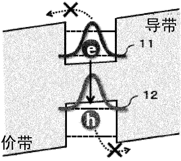
[0115] Next, ZnO having a lattice constant of 0.325 nm was laminated by a sputtering method to form barrier layer 5 . The film thickness of the barrier layer 5 was set to 30 nm. Next, on the barrier layer 5, ZnInON (composition ratio (element ratio) Zn:In=O:N=85:15, Zn+In:O+N=1:1) with a lattice constant of 0.329nm was combined The well layer 6 is grown to a film thickness of 30 nm. It is conside...
PUM
 Abstract
Description
Claims
Application Information