Sandwich parallel epitaxial gan pin type α irradiation cell and preparation method

A parallel and epitaxy technology, applied in the field of microelectronics, can solve the problems of large leakage current, easy introduction of surface defects, low energy conversion rate, etc.

Active Publication Date: 2017-02-15
XIDIAN UNIV
View PDF4 Cites 2 Cited by
  • Summary
  • Abstract
  • Description
  • Claims
  • Application Information

AI Technical Summary

Problems solved by technology

The substrate used in this structure is a P-type highly doped substrate, and the existing process of growing an epitaxial layer on the substrate is immature, so it is easy to introduce surface defects, the leakage current of the device is large, and the energy conversion rate is low.

Method used


Image

  • Sandwich parallel epitaxial gan pin type α irradiation cell and preparation method
  • Sandwich parallel epitaxial gan pin type α irradiation cell and preparation method
  • Sandwich parallel epitaxial gan pin type α irradiation cell and preparation method

Examples


Embodiment 1

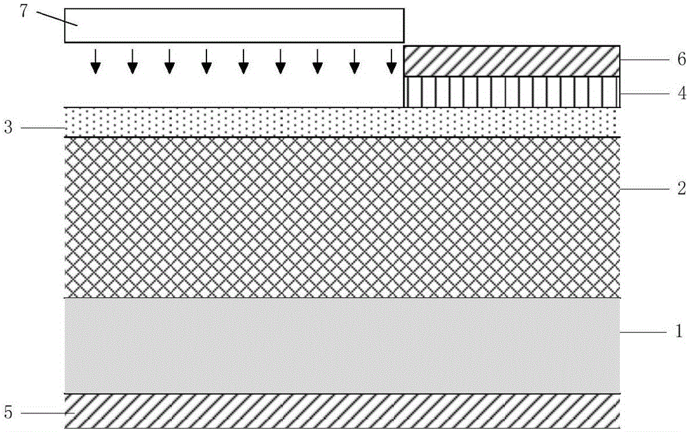
[0042] Embodiment 1, preparation α radiation source is Am 241 , PIN-type α-irradiated cell with sandwich parallel epitaxial GaN with α-radiation source layer thickness of 6 μm.

[0043] Step 1: Make the lower PIN knot.

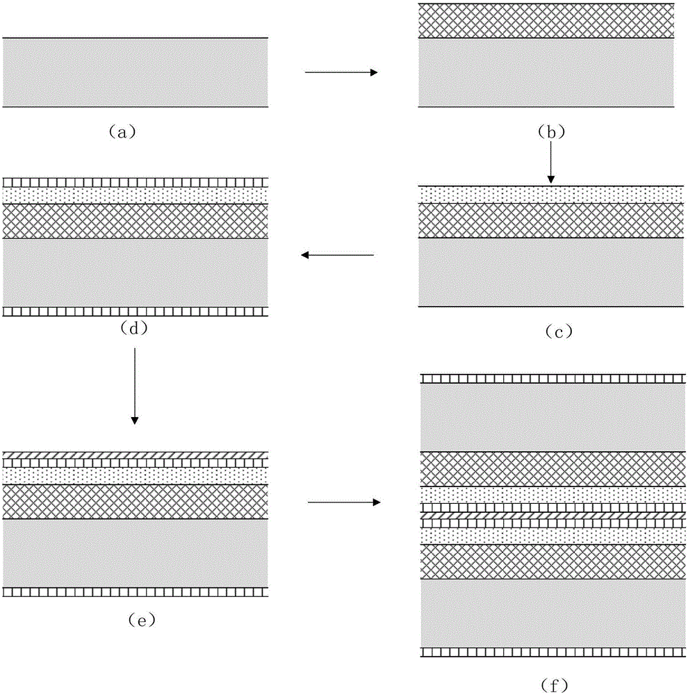
[0044] (1.1) Clean the 4H-SiC sample to remove surface pollutants, such as image 3 (a) shown.

[0045] (1.1.1) The doping concentration is l x 10 18 cm -3 Highly doped n-type 4H-SiC substrate sample in NH 4 OH+H 2 o 2 Soak the sample in the reagent for 10 minutes, take it out and dry it to remove the organic residue on the surface of the sample;

[0046] (1.1.2) Use HCl+H to remove the 4H-SiC sample after removing the surface organic residue 2 o 2 Soak the sample in the reagent for 10 minutes, take it out and dry it to remove ionic pollutants.

[0047] (1.2) Epitaxial growth of N-type low-doped SiC epitaxial layer, such as image 3 (b) shown.

[0048] A nitrogen-doped N-type doped epitaxial layer is epitaxially grown on the cleaned SiC sample by c...

Embodiment 2

[0062] Embodiment 2, preparation α radiation source is Am 241 , PIN-type α-irradiated cell with sandwich parallel epitaxial GaN with α-radiation source layer thickness of 4 μm.

[0063] Step 1: Make the lower PIN knot.

[0064] 1a) Clean the 4H-SiC sample to remove surface contaminants such as image 3 (a).

[0065] This step is the same as step (1.1) of Example 1.

[0066] 1b) Epitaxial growth of N-type low-doped SiC epitaxial layer, such as image 3 (b).

[0067] A nitrogen-doped N-type doped epitaxial layer is epitaxially grown on the cleaned SiC sample by chemical vapor deposition CVD. The process conditions are: epitaxy temperature is 1570°C, pressure is 100mbar, reaction gas is silane and propane, carrier gas is pure hydrogen, magazine source is liquid nitrogen, and the concentration of nitrogen doping is 2 x 10 15 cm -3 , growth of an N-type low-doped SiC epitaxial layer with a thickness of 25 μm.

[0068] 1c) Epitaxial growth of P-type highly doped GaN epitaxia...

Embodiment 3

[0078] Embodiment 3, preparation α radiation source is Pu 238 , PIN-type α-irradiated cells with sandwich parallel epitaxial GaN with a layer thickness of α-radiation source of 3 μm.

[0079] Step A: Make the upper PIN knot.

[0080] (A1) Clean the 4H-SiC sample to remove surface contaminants, such as image 3 (a).

[0081] This step is the same as step (1.1) of Example 1.

[0082] (A2) A nitrogen-doped N-type low-doped SiC epitaxial layer is epitaxially grown on the cleaned SiC sample by chemical vapor deposition CVD. The process conditions are as follows: the epitaxy temperature is 1570°C, the pressure is 100mbar, the reaction gas is silane and propane, the carrier gas is pure hydrogen, and the magazine source is liquid nitrogen. A nitrogen doping concentration of 3 x 10 15 cm -3 , a N-type low-doped SiC epitaxial layer with a thickness of 30 μm such as image 3 (b).

[0083] (A3) Put the sample after growing the N-type low-doped SiC epitaxial layer into the chemical...


PUM


Abstract

The invention discloses a sandwich parallel-type epitaxial GaN PIN-type alpha irradiation battery and a manufacturing method thereof. The sandwich parallel-type epitaxial GaN PIN-type alpha irradiation battery and the manufacturing method thereof mainly solve the problems that an existing nuclear battery is low in energy transformation ratio and output power. The sandwich parallel-type epitaxial GaN PIN-type alpha irradiation battery comprises an upper PIN junction, a lower PIN junction and an alpha radioactive source layer, wherein the upper PIN junction and the lower PIN junction are connected in parallel. The lower PIN junction sequentially comprises a P-type ohmic contact electrode, a P-type highly-doped GaN epitaxial layer, an N-type highly-doped 4H-SiC substrate, an N-type low-doped SiC epitaxial layer and an N-type ohmic contact electrode from top to bottom, and the bottom-to-top structure of the upper PIN junction is identical to the top-to-bottom structure of the lower PIN junction. The alpha radioactive source layer is clamped between the P-type ohmic contact electrode of the upper PIN junction and the P-type ohmic contact electrode of the lower PIN junction, so that high-energy beta particles are fully utilized. The sandwich parallel-type epitaxial GaN PIN-type alpha irradiation battery and the manufacturing method thereof have the advantages that the contact area of a radioactive source and a semiconductor is large, the nuclear raw material utilization rate and the energy harvesting rate are high, and the output voltage of the battery is large; the battery can supply electricity to a small circuit enduringly or to a polar region, a desert and other occasions.

Description

technical field [0001] The invention belongs to the field of microelectronics, and relates to a semiconductor device structure and preparation method, specifically a silicon carbide-based sandwich parallel epitaxial GaN PIN type α irradiation battery and a preparation method, which can be used for micro-nano electromechanical systems and other micro circuits And aerospace, deep sea, polar regions and other occasions that require long-term power supply and are unattended. [0002] technical background [0003] With people's demand for low power consumption, long life, high reliability and small size power supply equipment, as well as concerns about nuclear waste disposal, micronuclear batteries have become more and more popular. Due to its outstanding characteristics, micronuclear batteries can be used to solve the long-term power supply problems of micropipe robots, implanted microsystems, wireless sensor node networks, artificial cardiac pacemakers, and portable mobile elect...

Claims


Application Information

Patent Timeline
Patent Type & Authority Patents(China)
IPC IPC(8): G21H1/06
Inventor 郭辉赵亚秋宋庆文张艺蒙张玉明
Owner XIDIAN UNIV
Why Eureka
Try Eureka