Silicon solar cell and manufacturing method thereof

A silicon solar cell and silicon-based technology, applied in the field of solar cells, can solve the problems of low photoelectric conversion efficiency of solar cells, reduce the short-circuit current of solar cells, and reduce the efficiency of cells, etc., so as to enhance charge transport capacity, improve charge separation and transmission, etc. Performance, the effect of reducing the density of defect states

Active Publication Date: 2014-09-17
SUZHOU INAINK ELECTRONICS MATERIALS CO LTD
View PDF2 Cites 9 Cited by
  • Summary
  • Abstract
  • Description
  • Claims
  • Application Information

AI Technical Summary

Problems solved by technology

However, when the thickness of naturally occurring SiOx is too thick, this oxide layer will form a charge barrier, which hinders the transport of charges and simultaneously reduces the short-circuit current, open-circuit voltage, and fill factor of the solar cell, thereby reducing the efficiency of the cell.
Therefore, the photoelectric conversion efficiency of this type of solar cell is low, and the highest efficiency is only about 10%.

Method used


Image

  • Silicon solar cell and manufacturing method thereof
  • Silicon solar cell and manufacturing method thereof
  • Silicon solar cell and manufacturing method thereof

Examples


preparation example Construction

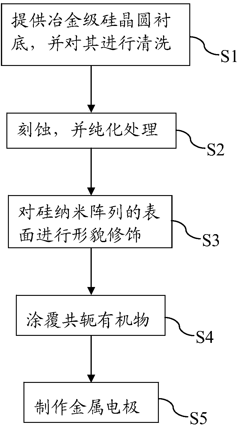
[0039] Such as figure 1 Shown, the present invention provides a kind of preparation method of silicon solar cell, it comprises the steps:

[0040] S1. Provide metallurgical grade silicon wafer substrates and clean the silicon wafer substrates;

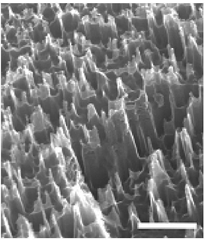
[0041] S2. Etching the cleaned metallurgical-grade silicon wafer substrate in an etching solution, and obtaining a regularly arranged silicon nano-array after purification;

[0042] S3. modifying the surface of the silicon nano-array to obtain a metallurgical-grade silicon nano-structure whose surface has been modified;

[0043]S4. Uniformly coat the conjugated organic matter on the surface of the obtained metallurgical grade silicon nanostructure, and perform annealing treatment after coating;

[0044] S5. Fabricate metal electrodes on the surface coated with the conjugated organic matter and the metallurgical grade silicon wafer substrate.

[0045] Wherein, the above step S2 specifically includes: putting the cleaned metallurgical...

Embodiment 1

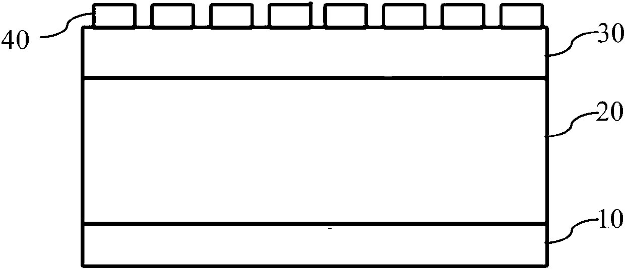
[0058] Such as image 3 , 4 As shown, provide a metallurgical grade silicon wafer, clean it, soak it in a diluted HF solution for at least 15 minutes, rinse it with deionized water and dry it with nitrogen, and put it in a glove box for use. Modification of metallurgical-grade silicon wafers with tetramethylammonium hydroxide. Then use PEDOT:PSS solution to spin-coat a layer of PEDOT:PSS film on the metallurgical grade silicon wafer at a speed of 9000 rpm, and then perform annealing treatment at 125°C. Then, under high vacuum conditions, an Ag electrode with a thickness of 200 nm is thermally evaporated on the PEDOT:PSS film, and an Al electrode is thermally evaporated on the back of the metallurgical grade silicon wafer to obtain the silicon solar cell of the present invention.

[0059] For the silicon solar cell prepared in this example, at room temperature, use a xenon lamp to simulate sunlight AM1.5, with a light intensity of 100mWcm -2 Under the conditions, the measure...

Embodiment 2

[0064] Such as Figure 7 Shown is the transmittance curves of metallurgical-grade silicon wafers with different thicknesses provided in this embodiment.

[0065] Provide metallurgical-grade silicon wafers of different thicknesses, soak metallurgical-grade silicon wafers of different thicknesses in diluted HF solution for at least 15 minutes, then rinse with deionized water and dry with nitrogen, and put them in the glove box for use. Modification of metallurgical-grade silicon wafers with tetramethylammonium hydroxide. Using the PEDOT:PSS solution, spin-coat a layer of PEDOT:PSS film on the silicon wafer at a speed of 9000 rpm, and then perform annealing treatment at 125°C. Then, an Ag electrode with a thickness of 200 nm is thermally evaporated on the PEDOT:PSS film under high vacuum conditions, and an Al electrode is thermally evaporated on the back of the silicon wafer to obtain the silicon solar cell of the present invention.

[0066] For the silicon solar cell prepared ...


PUM


Abstract

The invention discloses a silicon solar cell and a manufacturing method of the silicon solar cell. The manufacturing method of the silicon solar cell includes the following steps of firstly providing a metallurgical grade silicon wafer substrate and cleaning the metallurgical grade silicon wafer substrate, secondly etching the metallurgical grade silicon wafer substrate and conducting purification on the metallurgical grade silicon wafer substrate, thirdly conducting morphology modification on the surface of a silicon nanometer array, fourthly conducting morphology modification on the surface of the silicon nanometer array again, and fifthly coating the silicon nanometer array with conjugated organic matter. According to the manufacturing method of the silicon solar cell, the metallurgical grade silicon materials are applied to preparation of the solar cell, surface morphology treatment and surface purification treatment are conducted on the metallurgical grade silicon materials by fully applying the wet metal auxiliary chemical etching technology, and a silicon nanometer structure is formed. Passivating treatment is conducted on organic materials and the silicon nanometer structure, electrical performance and optical performance of a metallurgical grade silicon cell are improved, and charge separation performance and charge transmission performance are improved. Stability of the cell is improved through modification to organic-inorganic hybrid heterojunction, and the charge transmission capacity of the solar cell is enhanced.

Description

technical field [0001] The invention relates to the technical field of solar cells, in particular to a silicon solar cell and a preparation method thereof. Background technique [0002] With the continuous and rapid development of the global economy, oil, coal, natural gas and other non-renewable resources are decreasing day by day. Based on the concept of sustainable development, how to use renewable resources is becoming more and more important. There are many types of renewable resources, such as nuclear energy, solar energy, biomass energy, hydroelectric energy, wind energy, geothermal energy and tidal energy. Among many new energy sources, solar energy has become the focus of research and development and utilization of new energy due to its unique advantages such as abundant reserves, no geographical restrictions, clean and non-polluting, fastest growing, most environmentally friendly, and inexhaustible. With the development of science and technology, a series of sola...

Claims


Application Information

Patent Timeline
Patent Type & Authority Applications(China)
IPC IPC(8): H01L31/18H01L31/04
CPCY02E10/50H01L31/02363H01L31/04H01L31/1804H01L31/1868Y02E10/547Y02P70/50
Inventor 孙宝全张杰
Owner SUZHOU INAINK ELECTRONICS MATERIALS CO LTD
Why Eureka
Try Eureka