Radio frequency power amplifier

A radio frequency power and amplifier technology, applied in the field of semiconductor integrated circuits, can solve the problems of inability to achieve full-chip integration of radio frequency power amplifiers, low oxide breakdown voltage of CMOS devices, affecting the performance of power amplifiers, etc. The effect of improving integration and good frequency performance

Active Publication Date: 2014-11-19
SHANGHAI HUAHONG GRACE SEMICON MFG CORP
View PDF7 Cites 21 Cited by
  • Summary
  • Abstract
  • Description
  • Claims
  • Application Information

AI Technical Summary

Problems solved by technology

[0006] Although the high-frequency performance of the existing two-stage RF power amplifier realized by CMOS technology has been improved, it also brings some difficulties to the RF power amplifier, such as the breakdown voltage of the oxide layer of the CMOS device is too low, and the current driving ability is poor. , serious substrate coupling, etc.
In addition, the performance of on-chip passive devices is poor, especially the Q value of on-chip inductors is too low, which seriously affects the performance of power amplifiers. Therefore, components such as inductors often use off-chip methods, that is, the passive devices of RF power amplifiers implemented by existing CMOS processes such as Inductors and active devices such as CMOS devices often cannot be formed on the same chip, that is, the full chip integration of the entire RF power amplifier cannot be realized
Since the inductor needs to be manufactured off-chip, compared with a fully integrated RF power amplifier in which all components are integrated on the same chip, the cost of the existing RF power amplifier will be high and the application is inconvenient
[0007] except as figure 1 In addition to the RF power amplifiers realized by the existing CMOS process shown, the existing RF power amplifiers are also implemented by using gallium arsenide (GaAs) heterojunction bipolar transistors (HBT). Although GaAs HBT has better performance, it cannot Integrated with silicon (Si) process; in the field of semiconductor manufacturing, only silicon-based devices can achieve large-scale manufacturing, and GaAs HBT cannot be integrated with silicon process, so the cost is very high

Method used


Image

  • Radio frequency power amplifier
  • Radio frequency power amplifier

Examples


Embodiment Construction

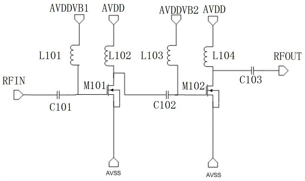
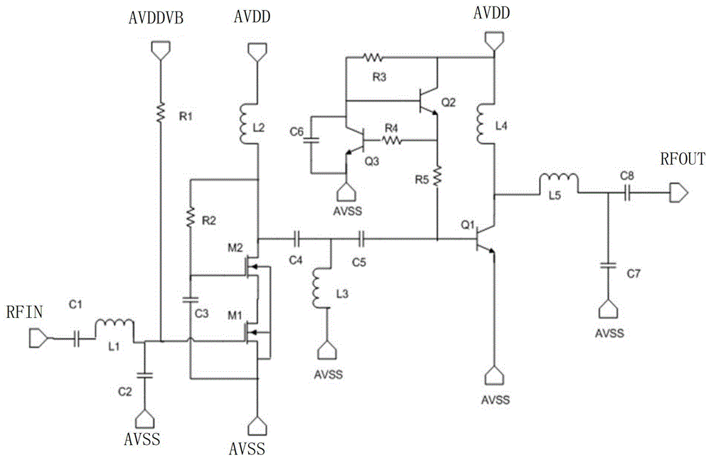
[0032] Such as figure 2 Shown is a radio frequency power amplifier in an embodiment of the present invention. The radio frequency power amplifier in the embodiment of the present invention is integrated on the same chip. The radio frequency power amplifier includes: an input matching network, a first-stage amplifying circuit, an inter-stage matching network, a second-stage amplifying circuit, an output matching network, and a second-stage bias Circuit.

[0033] The input matching network is connected between the radio frequency signal input terminal RFIN and the input terminal of the first stage amplifying circuit. In the embodiment of the present invention, the input matching network is an L-shaped matching network composed of a first inductor L1 and a second capacitor C2, and a DC blocking capacitor is provided between the radio frequency signal input terminal RFIN and the input matching network That is, the first capacitor C1. In other embodiments, the input matching netwo...


PUM


Abstract

The invention discloses a radio frequency power amplifier integrated on a same chip. The radio frequency power amplifier comprises two stages of amplifying circuits. An automatic biasing cascode CMOS amplifier is adopted in the first-stage amplifying circuit, and a SiGe HBT connected through a common emitter is adopted in the second-stage amplifying circuit. According to the radio frequency power amplifier, the withstand voltage, the isolation and the bandwidth of the circuits can be improved, the voltage swing and working current of the circuits can be improved, the gain and the maximum output power of the circuits can be improved, the frequency performance of the power amplifier can be improved, full-chip integration can be achieved, and accordingly, the integration degree is improved, cost is reduced, and the application is simplified.

Description

Technical field [0001] The invention relates to a semiconductor integrated circuit, in particular to a radio frequency power amplifier. Background technique [0002] In a wireless communication system, a radio frequency power amplifier is needed to receive and power amplify wireless signals. Such as figure 1 Shown is the existing two-stage RF power amplifier, including: [0003] The first-stage amplifier is composed of NMOS tube M101. The source of NMOS tube M101 is grounded. The radio frequency input signal RFIN is input to the gate of NMOS tube M101 through DC blocking capacitor C101. The bias voltage AVDDVB1 is added to the NMOS tube M101 through inductor L1. The gate and the drain of the NMOS tube M101 are connected to the power supply voltage through the choke inductor L2. [0004] The second stage amplifier is composed of NMOS tube M102. The source of NMOS tube M102 is grounded. The gate of NMOS tube M102 is connected to the drain of NMOS tube M101 through isolation capacitor...

Claims


Application Information

Patent Timeline
Patent Type & Authority Applications(China)
IPC IPC(8): H03F3/189H03F1/42
Inventor 刘国军朱红卫唐敏赵郁炜
Owner SHANGHAI HUAHONG GRACE SEMICON MFG CORP
Why Eureka
Try Eureka