Organic light emission diode, display screen and terminal

An electroluminescence device and electroluminescence technology, which are applied in the field of electric light sources, can solve the problems of reducing the reflectivity of OLEDs, difficult to ensure uniformity, and unsatisfactory reflectivity, and achieve uniform film layers, low driving current, and low cost. Effect

Inactive Publication Date: 2014-12-03
OCEANS KING LIGHTING SCI&TECH CO LTD +2
View PDF5 Cites 5 Cited by
  • Summary
  • Abstract
  • Description
  • Claims
  • Application Information

AI Technical Summary

Problems solved by technology

[0006] In order to reduce the reflectivity of OLED, people have also made some explorations and achieved certain results, such as the use of organic materials Alq 3 1. TPBi material is used as the dielectric layer. Although the material is easy to form a film and has a certain light transmittance, its electrical conductivity is not strong. Therefore, only a thinner dielectric layer can be prepared, usually with a thickness below 5nm. Avoiding an increase in drive voltage due to excessive thickness
However, for the large-area preparation of OLEDs, this extremely thin thickness requires precise control during the preparation process, and its uniformity is difficult to guarantee. In order to achieve a uniform film layer, very precise monitoring equipment and high-precision Evaporation equipment
As a result, the production cost of OLED is increased invisibly, and the yield rate is low
In addition, the organic material Alq 3 , TPBi material as a dielectric layer can only reduce reflection for a specific wavelength of light such as 550nm wavelength, and has almost no effect on light of other wavelengths, so its reflectivity is still not ideal

Method used


Image

  • Organic light emission diode, display screen and terminal
  • Organic light emission diode, display screen and terminal
  • Organic light emission diode, display screen and terminal

Examples


preparation example Construction

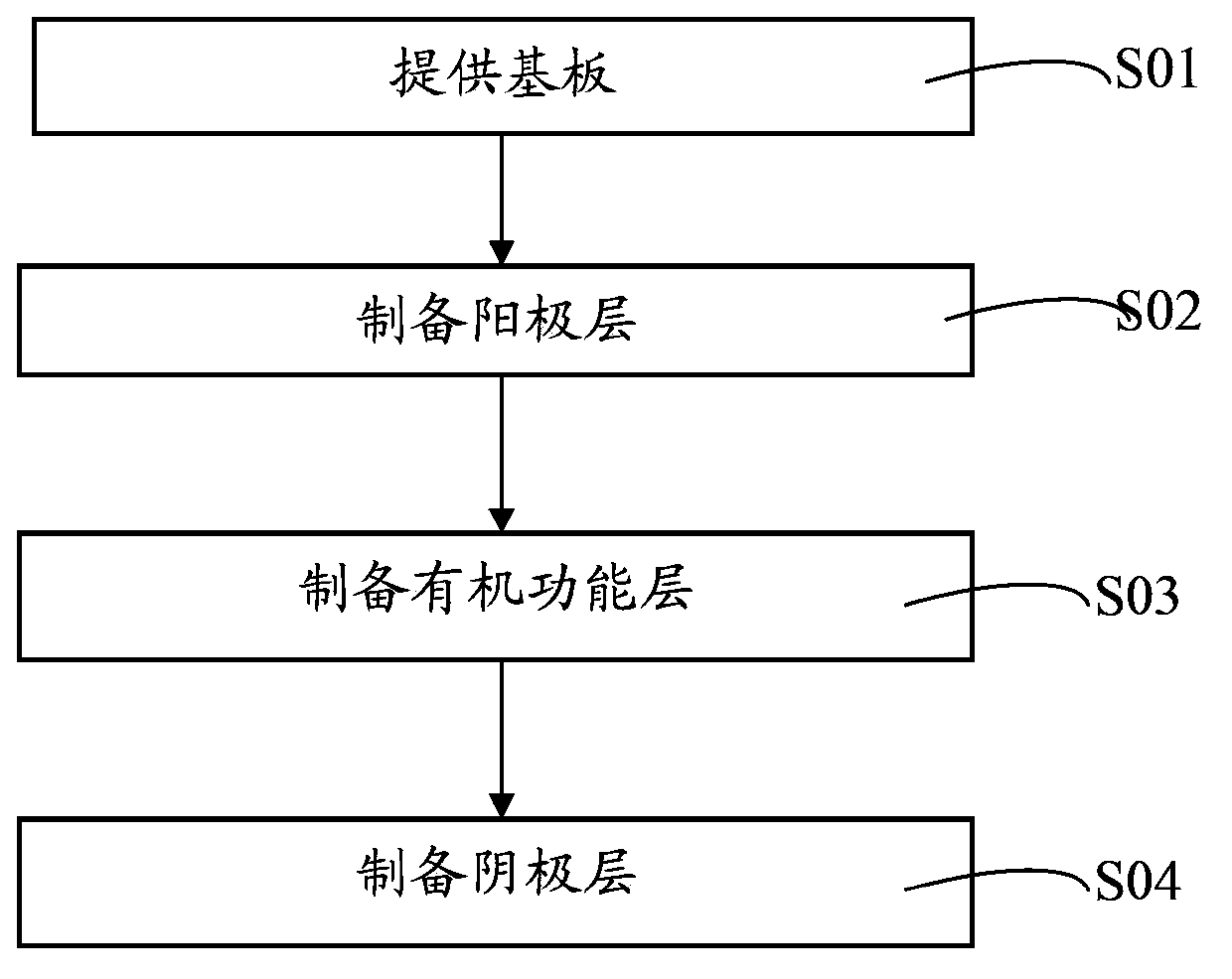
[0048] Correspondingly, the preparation method of the organic electroluminescent device of the above-mentioned embodiment can be as follows image 3 So show. Process preparation, see also Figure 1~2 , Its preparation method includes the following steps:

[0049] S01. Provide a transparent substrate 1;

[0050] S02. Preparation of the anode layer 2: In a vacuum system, the transparent conductive oxide is magnetron sputtered to prepare the anode layer 2 on the surface of the substrate 1 in step S01;

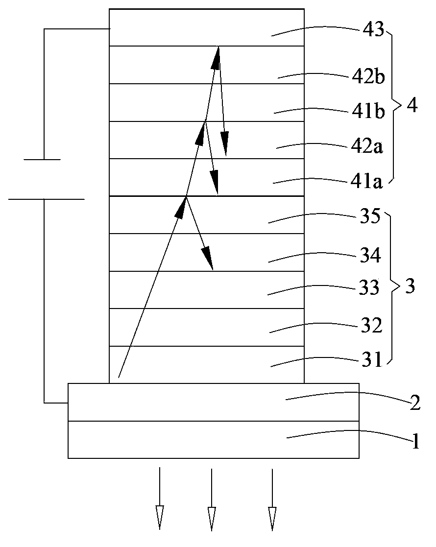
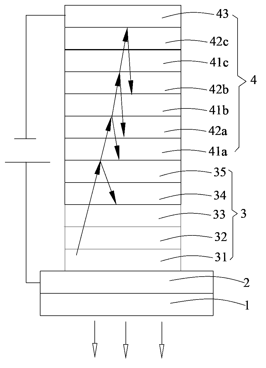
[0051] S03. Preparation of organic functional layer 3: In step S02, a hole injection layer 31, a hole transport layer 32, a light emitting layer 33, and an electron transport layer are sequentially evaporated on the surface of the anode layer 2 opposite to the bonding surface of the light-transmitting substrate layer 1 34. The electron injection layer 35 forms the organic functional layer 3;

[0052] S04. Preparation of the cathode layer 4: In the vacuum coating system, the semi-permeab...

Embodiment 1

[0068] An organic electroluminescence device with a low reflectivity cathode and an anode as the light-emitting surface. Its structure is: glass substrate / ITO (70nm) / hole injection layer (CuPc, 20nm) / hole transport layer (NPB, 40nm) ) / Luminescent layer (Alq 3 :C545T(10%),10nm) / electron transport layer (TPBi,40nm) / electron injection layer (LiF,1nm) / Cr(10nm) / Alq 3 :Li 2 CO 3 (60nm) / Cr(10nm) / Alq 3 :Li 2 CO 3 (80nm) / Ag(100nm). Among them, Cr(10nm) / Alq 3 :Li 2 CO 3 (60nm) / Cr(10nm) / Alq 3 :Li 2 CO 3 (80nm) / Ag(100nm) constitutes the anode, and the Cr layer is a semi-permeable metal layer, Alq 3 :Li 2 CO 3 The layer is an interference layer, and Ag (100nm) is a metal reflective layer.

[0069] The preparation method is as follows:

[0070] (1) When the vacuum degree is 10 -4 Prepared in the Pa vacuum coating system, the glass substrate is cleaned with a cleaning agent, then with distilled water, acetone, followed by ultrasonic cleaning, and then in the coating system;

[0071] (2) First, pre...

Embodiment 2

[0076] An organic electroluminescence device with a low reflectivity cathode and an anode as the light-emitting surface. Its structure is: glass substrate / ITO (100nm) / hole injection layer (CuPc, 20nm) / hole transport layer (NPB, 40nm) ) / Luminescent layer (Alq 3 :C545T(10%),10nm) / electron transport layer (TPBi,40nm) / electron injection layer (LiF,1nm) / Al(7nm) / TPBi:Cs 2 CO 3 (20nm) / Al(7nm) / TPBi:Cs 2 CO 3 (30nm) / Al(7nm) / TPBi:Cs 2 CO 3 (40nm) / Mg-Al(70nm). Among them, Al(7nm) / TPBi:Cs 2 CO 3 (20nm) / Al(7nm) / TPBi:Cs 2 CO 3 (30nm) / Al(7nm) / TPBi:Cs 2 CO 3 (40nm) / Mg-Al (70nm) constitutes the anode, and the Al layer is a semi-permeable metal layer, TPBi:Cs 2 CO 3 The layer is an interference layer, and Mg-Al (70nm) is a metal reflective layer.

[0077] The preparation method is as follows:

[0078] (1) When the vacuum degree is 10 -4 Prepared in the Pa vacuum coating system, the glass substrate is cleaned with a cleaning agent, then with distilled water, acetone, followed by ultrasonic cleaning, ...


PUM


Abstract

The invention discloses an organic light emission diode, a display screen and a terminal. The organic light emission diode includes a transmitting substrate, an anode layer, an organic function layer and a cathode layer, which are sequentially laminated and combined. The cathode layer includes a metal reflection layer, at least two interference layers and at least two transflective metal layers. The interferences layers and the transflective metal layers are alternatively laminated and combined between the metal reflection layer and the organic function layer. The interference layers and the metal reflection layers are laminated and combined. The transflective metal layer and the organic function layer are laminated and combined, wherein the material of the interference layers includes an organic electron transmission material and an alkali metal compound doped therein, and the mass of the alkali metal compound is 5-50% of the total mass of the interference layers. The cathode of the organic light emission diode effectively reduces a light reflectivity of the cathode of the organic light emission diode and improves the contrast ratio thereof. The display screen which includes the organic light emission diode, and the terminal have high contrast ratios and clear display pictures.

Description

Technical field [0001] The invention belongs to the technical field of electric light sources, and specifically relates to an organic electroluminescence device, a display screen and a terminal thereof. Background technique [0002] Organic Light Emission Diode (Organic Light Emission Diode, hereinafter referred to as OLED) is a current-type semiconductor light-emitting device based on organic materials. Its typical structure is to make a layer of tens of nanometers thick organic light-emitting material as the light-emitting layer on ITO glass, and there is a layer of low work function metal electrode above the light-emitting layer. [0003] The light-emitting principle of OLED is based on the fact that electrons are injected from the cathode to the lowest unoccupied molecular orbital (LUMO) of organic matter under the action of an external electric field, and holes are injected from the anode to the highest occupied orbital (HOMO) of organic matter. Electrons and holes meet and r...

Claims


Application Information

Patent Timeline
Patent Type & Authority Applications(China)
IPC IPC(8): H01L51/50H01L51/52
CPCH10K50/82H10K50/865H10K2102/00
Inventor 周明杰冯小明黄辉王平
Owner OCEANS KING LIGHTING SCI&TECH CO LTD
Why Eureka
Try Eureka