Organic light emitting device and manufacturing method thereof

An electroluminescent device and electroluminescent technology, which are applied in the fields of electro-solid devices, semiconductor/solid-state device manufacturing, electrical components, etc., can solve problems such as low luminous efficiency, and achieve the effects of improving luminous efficiency, speed and matching.

Inactive Publication Date: 2014-12-03
OCEANS KING LIGHTING SCI&TECH CO LTD +2
View PDF6 Cites 2 Cited by
  • Summary
  • Abstract
  • Description
  • Claims
  • Application Information

AI Technical Summary

Problems solved by technology

However, in current organic electroluminescent devices, the transport rate of holes is much lower than that of electrons, resulting in low luminous efficiency of organic electroluminescent devices.

Method used


Image

  • Organic light emitting device and manufacturing method thereof
  • Organic light emitting device and manufacturing method thereof
  • Organic light emitting device and manufacturing method thereof

Examples


preparation example Construction

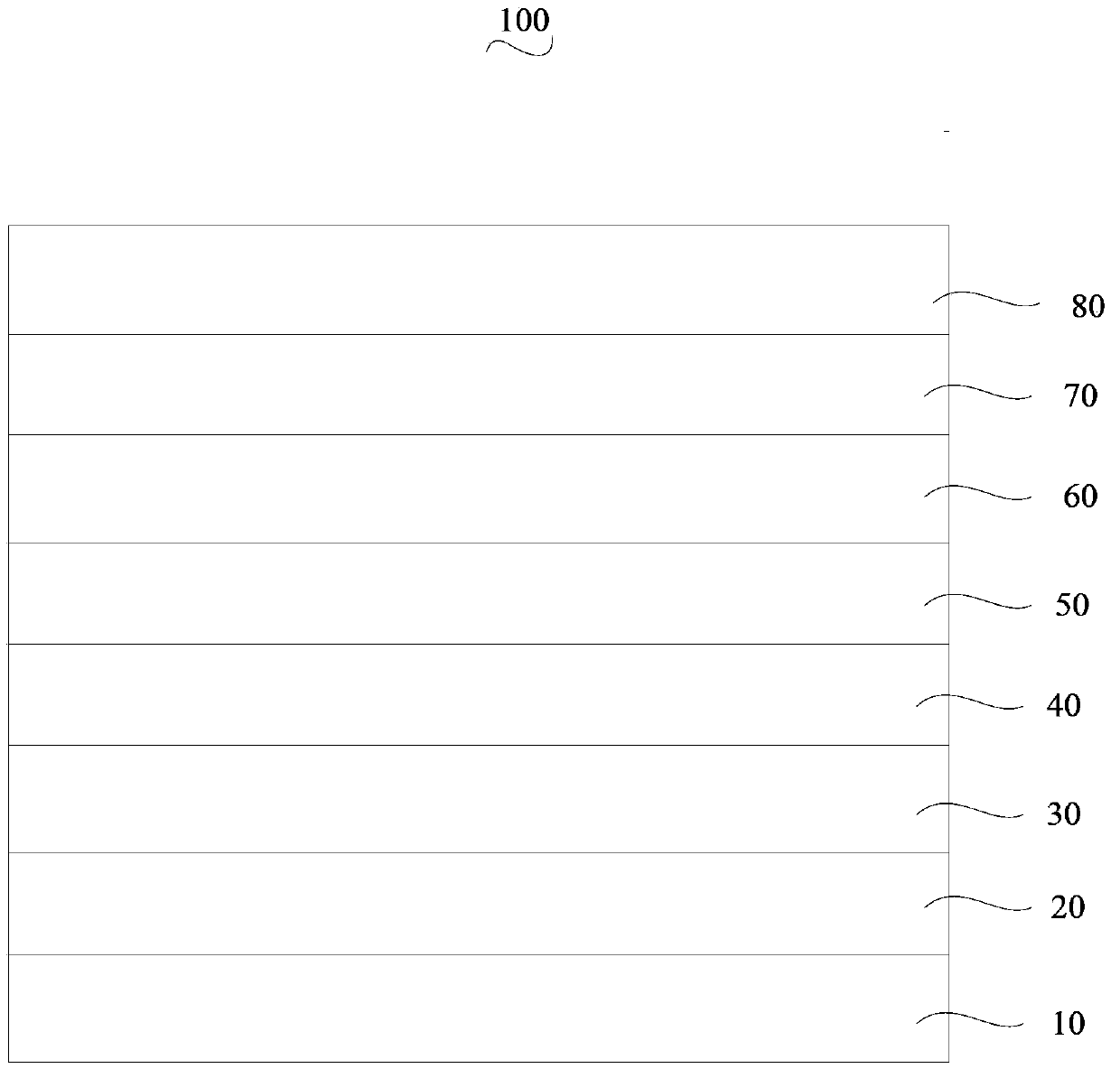
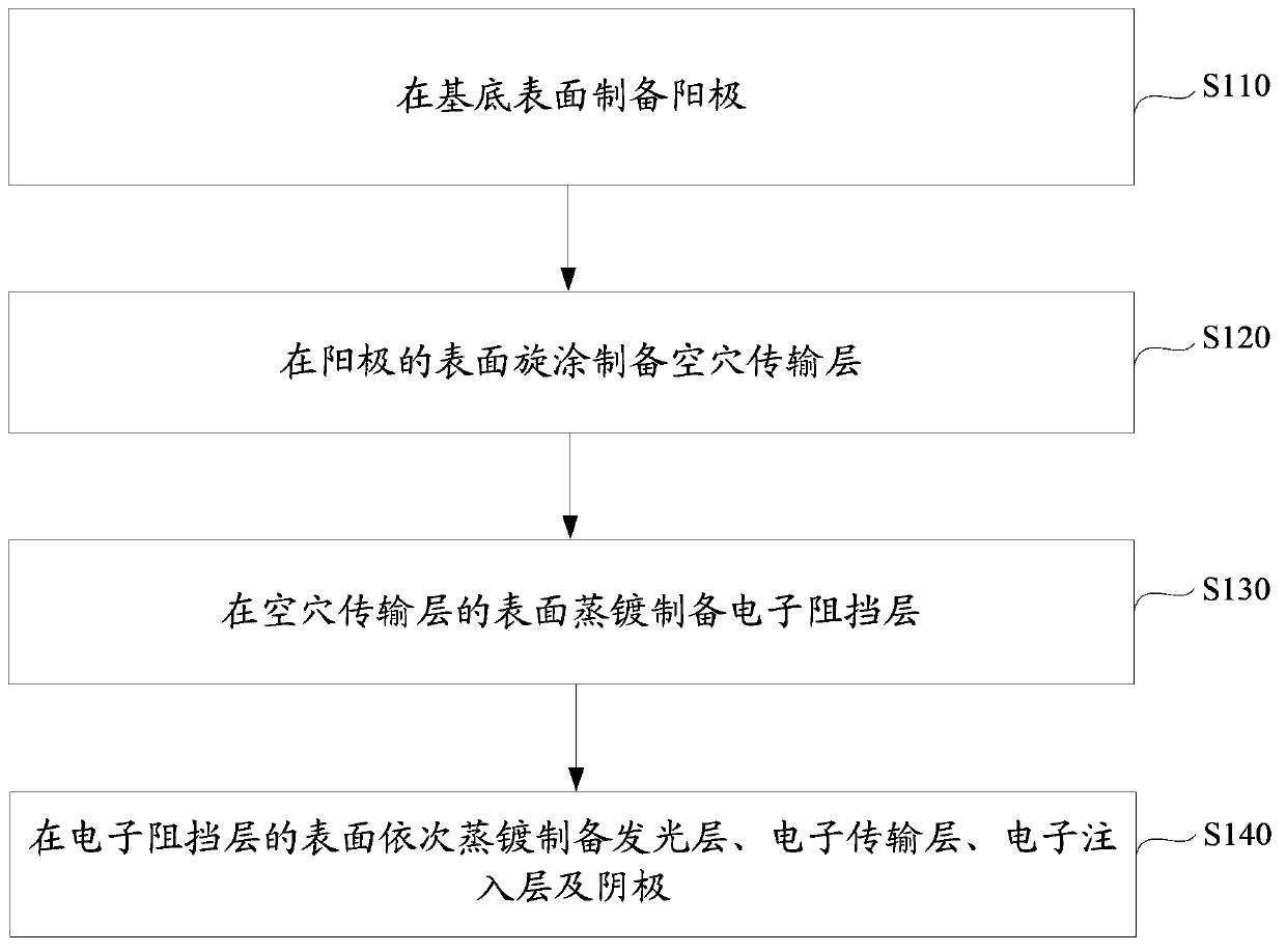
[0033] Such as figure 2 Shown, the preparation method of the organic electroluminescent device of one embodiment, comprises the following steps:

[0034] Step S110 , preparing an anode 20 on the surface of the substrate 10 .

[0035] The substrate 10 is glass. The thickness of the substrate 10 is 0.1 mm˜1 mm.

[0036] The substrate 10 is pre-treated before use, and the pre-treatment includes: placing the substrate in deionized water containing detergent for ultrasonic cleaning, after cleaning, it is treated with isopropanol and acetone in ultrasonic waves for 20 minutes, and then nitrogen gas is used to clean the substrate. blow dry.

[0037] The anode 20 is formed on the surface of the substrate 10 . The material of the anode 20 is indium tin oxide (ITO) or aluminum doped zinc oxide (AZO). The thickness of the anode 20 is 70nm-200nm.

[0038] In this embodiment, the anode 20 is prepared by vacuum sputtering. When sputtering, the background vacuum is 1×10 -5 Pa~1×10 ...
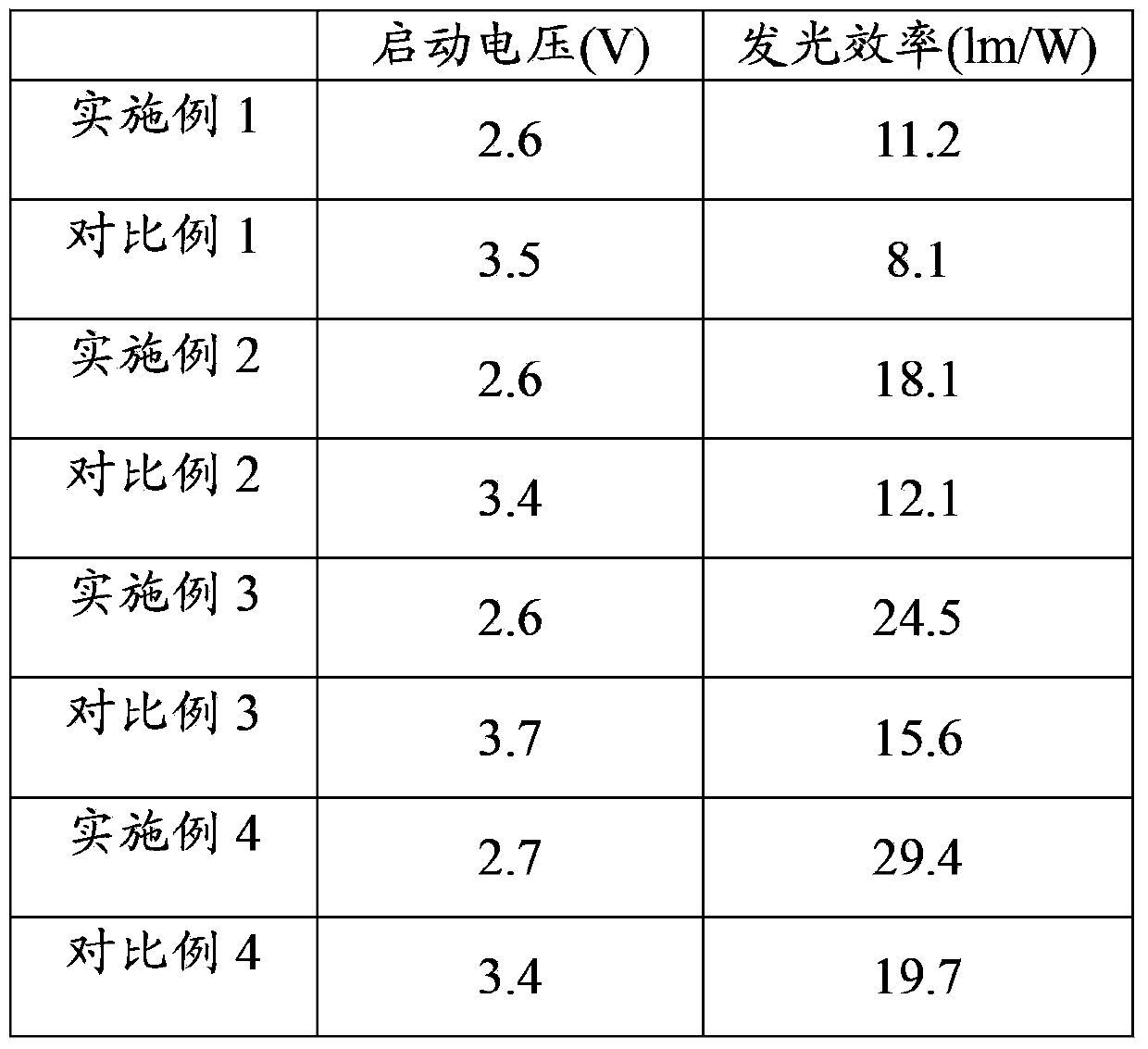
Embodiment 1

[0062] The structure of the organic electroluminescent device in this embodiment is: glass substrate / ITO (70nm) / F4-TCNQ: P3HT (50nm) / TPD (5nm) / Rubrene (10nm) / TPBi (20nm) / LiF (0.5nm) / Ag(200nm). Wherein, " / " indicates a stacked structure, and ":" indicates doping or mixing, and the following embodiments are the same.

[0063] The preparation of the organic electroluminescent device of this embodiment is as follows:

[0064]Step 1. Provide the substrate, put the glass in deionized water containing detergent for ultrasonic cleaning, after cleaning, use isopropanol and acetone in ultrasonic treatment for 20 minutes, and then blow dry with nitrogen;

[0065] Step 2. In a vacuum of 1×10 -5 In the vacuum coating system of Pa, the anode is prepared on the substrate by magnetron sputtering, the material is ITO, and the thickness is 70nm;

[0066] Step 3, using a spin-coating process to prepare a hole transport layer on the surface of the anode under a nitrogen atmosphere,

[0067] ...

Embodiment 2

[0076] The structure of the organic electroluminescent device in this embodiment is: glass substrate / AZO(200nm) / F6-TNAP:P3HT(1:10000) / TCTA(10nm) / Ir(piq) 3 :NPB(8%, 20nm) / Bphen(60nm) / NaF(2nm) / Al(70nm).

[0077] The preparation of the organic electroluminescent device of this embodiment is as follows:

[0078] Step 1, providing a base;

[0079] Step 2. In a vacuum of 1×10 -3 In the vacuum coating system of Pa, the method of magnetron sputtering is used to prepare an anode on the substrate, the material is AZO, and the thickness is 200nm;

[0080] Step 3, using a spin-coating process to prepare a hole transport layer on the surface of the anode under a nitrogen atmosphere,

[0081] The material of the hole transport layer is F6-TNAP doped P3HT, the molar ratio is 1:10000, and it is prepared according to the following method:

[0082] 1. Dissolve the dopant F6-TNAP and poly-3-hexylthiophene with the solvent dimethyl sulfoxide according to the metering ratio, and stir evenly, w...


PUM


Abstract

The invention discloses an organic light emitting device, which comprises a substrate, an anode, a hole transmission layer, an electron blocking layer, a light emitting layer, an electron transmission layer, an electron injection layer and a cathode stacked sequentially. Material of the hole transmission layer comprises poly-3-hexylthiophene and a dopant doped in the poly-3-hexylthiophene, wherein the dopant is at least one selected from 2, 3, 5, 6-tetrafluoro-7, 7 ', 8, 8'-tetracyanoquino-dimethane, 1, 3, 4, 5, 7, 8-hexafluoride-tetracyano-dimethyl naphthalene quinine, 2, 2'-(2, 5-dicyano-3, 6-difluorocyclohexane-2, 5-diene-1, 4-di idene) di-malononitrile and 2, 3, 6, 7, 10, 11-hexacyano-1, 4, 5, 8, 9, 12-hexaazatriphenylene. The light emitting efficiency of the organic light emitting device is high. The invention also provides an organic light emitting device manufacturing method.

Description

technical field [0001] The invention relates to the field of electronic devices, in particular to an organic electroluminescent device and a preparation method thereof. Background technique [0002] The luminescence principle of organic electroluminescent devices is based on the action of an external electric field, electrons are injected from the cathode to the lowest unoccupied molecular orbital (LUMO) of organic matter, and holes are injected from the anode to the highest occupied molecular orbital (HOMO) of organic matter. Electrons and holes meet, recombine, and form excitons in the light-emitting layer. Excitons migrate under the action of an electric field, transfer energy to the light-emitting material, and excite electrons to transition from the ground state to the excited state. The excited state energy is deactivated by radiation to generate photons , releasing light energy. However, in current organic electroluminescent devices, the transport rate of holes is mu...

Claims


Application Information

Patent Timeline
Patent Type & Authority Applications(China)
IPC IPC(8): H01L51/50H01L51/54H01L51/56
CPCH10K85/113H10K85/649H10K50/155H10K50/18H10K71/00
Inventor 周明杰冯小明张娟娟王平
Owner OCEANS KING LIGHTING SCI&TECH CO LTD
Why Eureka
Try Eureka