A kind of forming method of graphene pattern
A graphene and graphene layer technology, applied in gaseous chemical plating, coatings, electrical components, etc., can solve problems such as high cost, complex template manufacturing process, and difficulty in achieving accurate positioning of graphene, reducing costs, Avoid quality defects and avoid the effect of repeated transfers
- Summary
- Abstract
- Description
- Claims
- Application Information
AI Technical Summary
Problems solved by technology
Method used
Image
Examples
Embodiment 1
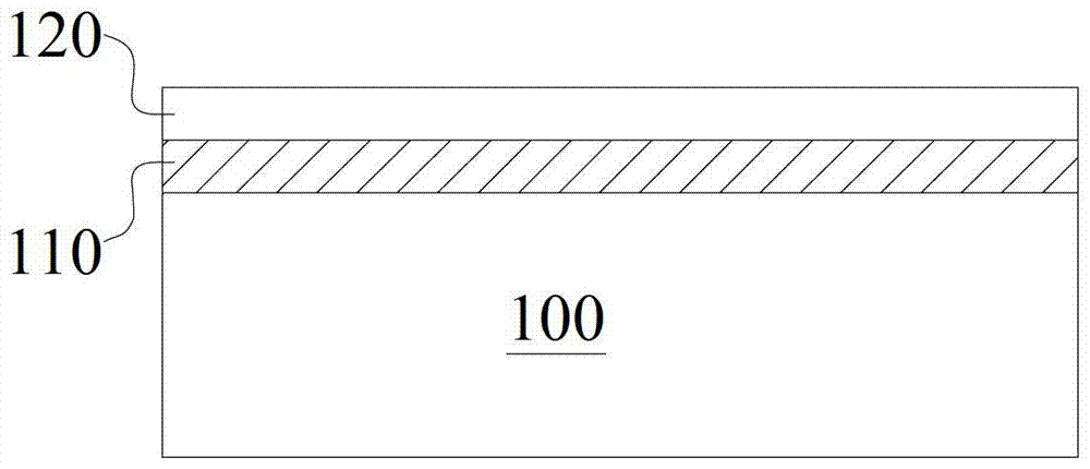
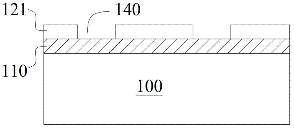
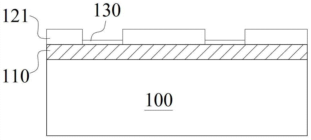
[0049] Figure 1~4 It is a schematic diagram of Embodiment 1 of the first method for forming a graphene pattern provided by the present invention.
[0050] refer to figure 1 , providing a substrate 100; on the substrate 100, a graphene growth layer 110 and a masking layer 120 are successively formed from bottom to top.
[0051] In this embodiment, the substrate 100 may be silicon, germanium, gallium arsenide or silicon germanium (SiGe) compound with single crystal, polycrystalline or amorphous structure, or a substrate made of silicon on insulator (SOI). All existing substrates can be used as the substrate of the present invention, and will not be listed here. In this embodiment, the substrate 100 may be a silicon substrate.
[0052] In this embodiment, the graphene growth layer 110 is preferably a silicon carbide layer. The method for forming the silicon carbide layer may be an epitaxial method, and the specific process includes: placing the substrate 100 in a CVD chamber...
Embodiment 2
[0065] In this embodiment, the graphene layer is also formed by the thermal decomposition method of silicon carbide. Compared with the technical solution in the above-mentioned embodiment 1, the only difference is that in this embodiment, the substrate is silicon carbide, and graphite is directly formed on the substrate. vinyl layer.
[0066] Figure 5-7 It is a schematic diagram of the forming method of the graphene pattern of the present embodiment, and its specific steps include:
[0067] refer to Figure 5 , providing a substrate 200 , and forming a masking pattern layer 123 on the substrate 200 .
[0068] In this embodiment, the substrate 200 is a silicon carbide substrate.
[0069] In this embodiment, the masking pattern layer 123 has an opening 142 , and the surface of the silicon carbide substrate 200 is exposed in the opening 142 . Wherein, the forming process of the masking pattern layer 123 is similar to the forming process of the masking pattern layer 121 in Em...
Embodiment 3
[0073] The present invention also provides another method for forming a graphene pattern, which differs from the technical scheme of the method for forming a graphene pattern listed in Examples 1 and 2 in that the method for forming a graphene pattern is formed on a substrate with After exposing the masking pattern layer of the opening of the substrate, a graphene growth layer is formed on the surface of the substrate in the opening, so that a graphene layer is formed on the surface of the graphene growth layer. The method for forming the graphene pattern provided in this embodiment also defines the subsequent graphene layer structure with the opening structure of the masking pattern layer, so as to avoid the graphene layer being damaged by etching in the further patterning process after the graphene layer is formed. are damaged, thereby ensuring the electrical properties of the formed graphene pattern. Moreover, after the graphene layer is formed, it is not necessary to remov...
PUM
| Property | Measurement | Unit |
|---|---|---|
| thickness | aaaaa | aaaaa |
| electrical resistivity | aaaaa | aaaaa |
Abstract
Description
Claims
Application Information


