Method for improving light extraction efficiency of light-emitting diode by means of nanoindentations

A technology of light-emitting diodes and light extraction efficiency, which is applied in the direction of semiconductor devices, electrical components, circuits, etc., can solve the problems of long processing time, high use cost, and limited improvement of light extraction efficiency, so as to facilitate large-scale manufacturing and economical use Guaranteed effect on cost and quality

Inactive Publication Date: 2014-12-24
SHANDONG UNIV
View PDF4 Cites 5 Cited by
  • Summary
  • Abstract
  • Description
  • Claims
  • Application Information

AI Technical Summary

Problems solved by technology

The roughening of the surface of light-emitting diodes by etching has the following disadvantages: 1. The ions used in plasma etching have an impact on the doping ratio of semiconductor materials, resulting in changes in the quantum properties of semiconductors and affecting electrical properties; 2. Plasma Etching equipment is expensive and the cost of use is high, which greatly increases the manufacturing cost of light-emitting diodes. 3. Etching has no control over the roughened morphology and size of the semiconductor surface, and cannot be optimized
4. The processing time is long, which is not conducive to large-scale production
The disadvantages of the above two methods are: 1. The electron beam exposure equipment is expensive for several phases, and the single processing are...

Method used


Image

  • Method for improving light extraction efficiency of light-emitting diode by means of nanoindentations
  • Method for improving light extraction efficiency of light-emitting diode by means of nanoindentations
  • Method for improving light extraction efficiency of light-emitting diode by means of nanoindentations

Examples


Embodiment 1

[0047] A method for improving the light extraction efficiency of a light-emitting diode by using nano-indentation, the method comprising:

[0048] Using the nano-scale patterned sapphire substrate as a template, by applying a load to the nano-scale patterned sapphire substrate and the light-emitting diode epitaxial wafer, under the action of the external force of the load, the nano-scale patterned structure on the sapphire substrate acts as an indenter. into the gallium phosphide window layer of the light emitting diode epitaxial wafer, and obtain a periodic nanoscale patterned indentation structure on the gallium phosphide window layer of the light emitting diode epitaxial wafer. The light extraction efficiency of the light emitting diode is thus increased.

Embodiment 2

[0050] A method for improving the light extraction efficiency of light-emitting diodes by using nano-indentation as described in Example 1, including the following specific steps:

[0051] ① Ultrasonic cleaning of nanoscale patterned sapphire substrate and LED epitaxial wafer to ensure their respective surfaces are clean;

[0052] ②Using the nano-scale patterned sapphire substrate as a nano-indentation template, attaching the side of the sapphire substrate with a nano-scale patterned structure to the upper surface of the light-emitting diode epitaxial wafer;

[0053] ③ Applying pressure to the nano-scale patterned sapphire substrate and the light-emitting diode epitaxial wafer, the direction of the loading pressure is the direction perpendicular to the surface of the light-emitting diode, so that the nano-scale patterned structure on the surface of the sapphire substrate acts as an indenter Pressing into the light-emitting diode epitaxial wafer, forming a nano-scale patterned ...

Embodiment 3

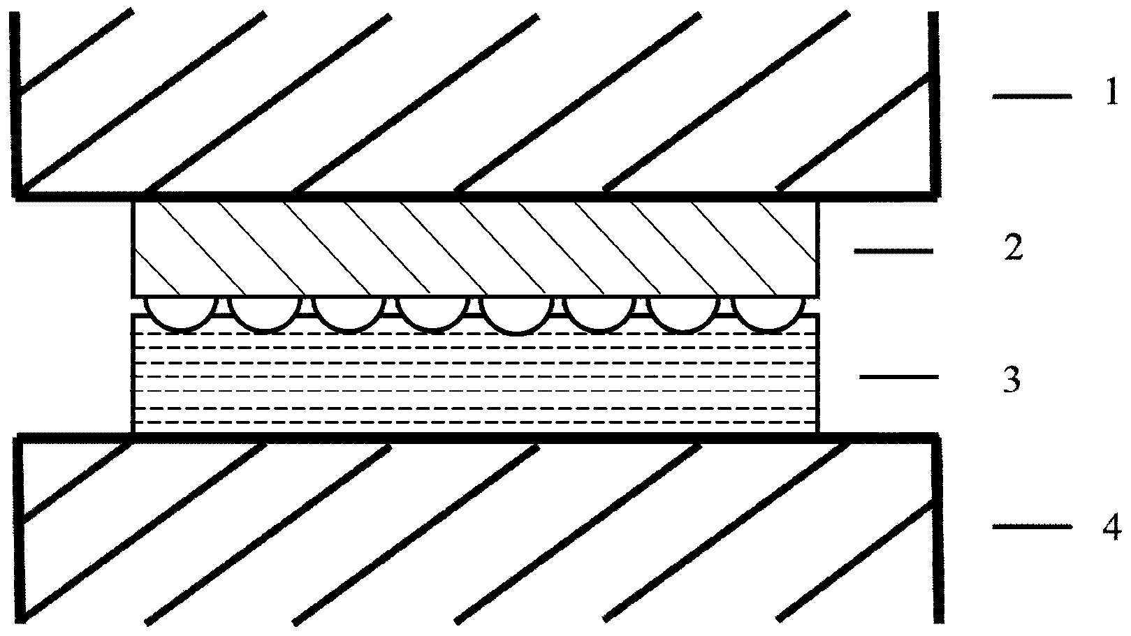
[0056] Such as Figure 1-Figure 4 shown.

[0057] Using the method described in Examples 1 and 2 to carry out nano-indentation treatment on the AlGaInP red light-emitting diode epitaxial wafer, the steps are as follows:

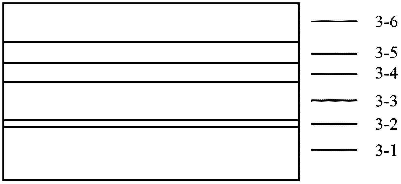
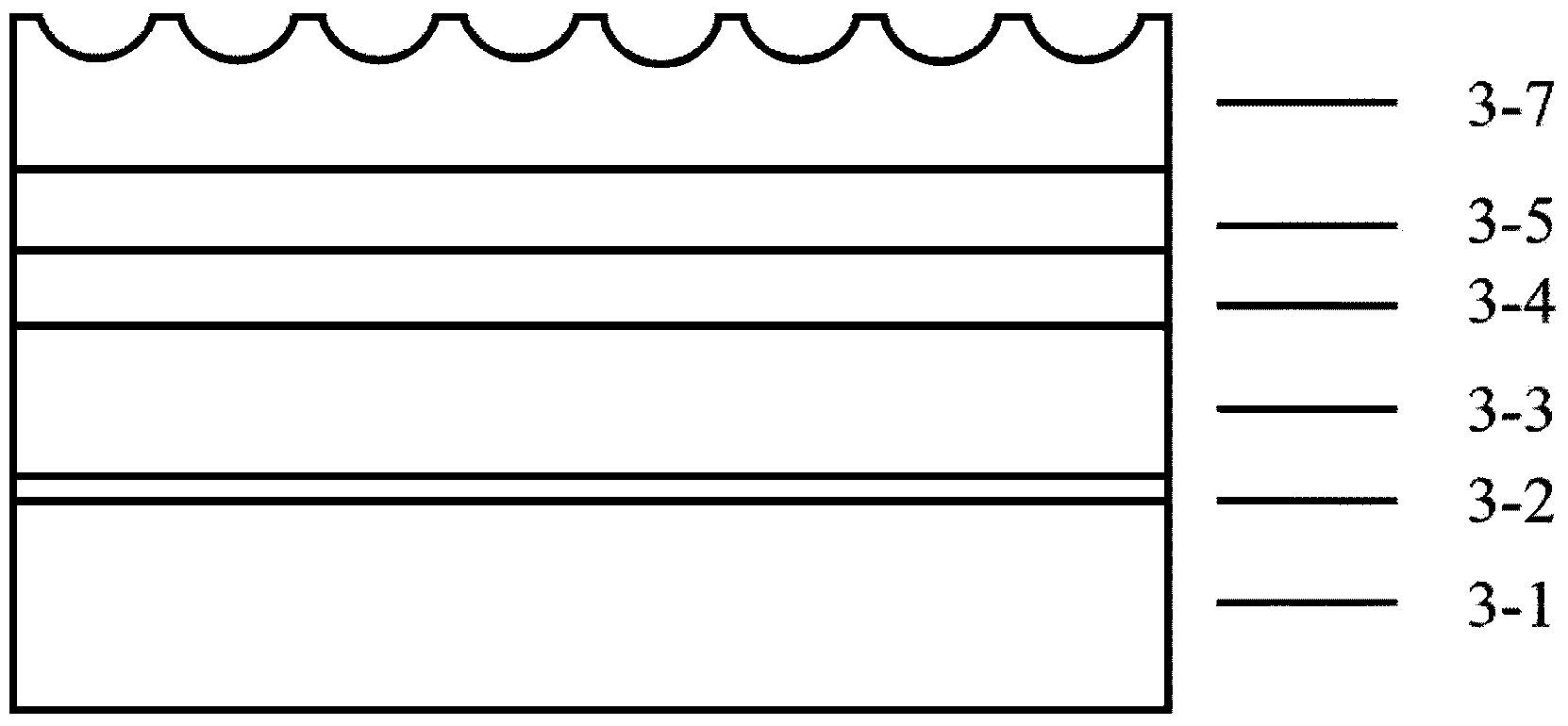
[0058] (1) Growth of red light-emitting diode epitaxial wafers: Bragg reflector 3-2, n-type aluminum gallium indium phosphorus layer 3-3, and multiple quantum wells are sequentially grown on the surface of GaAs substrate 3-1 by metalorganic chemical vapor deposition Layer 3-4, p-type aluminum gallium indium phosphide layer 3-5 and p-type GaP layer 3-6 are prepared into a red light emitting diode epitaxial wafer;

[0059] (2) Preparation of nanoscale patterned sapphire substrate 2: form a mask layer on the surface of the sapphire substrate, pattern the mask layer, and use ICP etching to obtain a hemispherical patterned structure on the surface of the sapphire substrate;

[0060] (3) Utilizing the nanoscale patterned sapphire substrate in step (2) as a nano-i...


PUM

PropertyMeasurementUnit
Young's modulusaaaaaaaaaa

Abstract

The invention provides a method for improving the light extraction efficiency of a light-emitting diode by means of nanoindentations. According to the method for improving the light extraction efficiency of the light-emitting diode by means of the nanoindentations, a nanoscale patterned sapphire substrate is taken as a template, a large area of periodical nanoindentation structures are formed on a gallium phoshpide window layer of an epitaxial wafer of the light-emitting diode by exerting loads on the patterned sapphire substrate and the epitaxial wafer of the light-emitting diode, and thus the light extraction efficiency of the light-emitting diode is improved. According to the method for improving the light extraction efficiency of the light-emitting diode by means of the nanoindentations, the sizes, the shapes and the periods of the periodical nanoindentation structures formed on the gallium phoshpide window layer of the epitaxial wafer of the light-emitting diode can be effectively controlled by adjusting the shape and the period of the patterned sapphire substrate and the loads. Compared with an existing manufacturing technology, the method for improving the light extraction efficiency of the light-emitting diode by means of the nanoindentations has the advantages that operation is easy, cost is extremely low, and a large area of good nanoindentations can be formed on the surface of the epitaxial wafer of the light-emitting diode rapidly.

Description

technical field [0001] The invention relates to a method for improving the light extraction efficiency of a light-emitting diode by using nano-indentation, and belongs to the field of semiconductor optoelectronic material device preparation. Background technique [0002] In recent years, the market of light-emitting diodes (LEDs) has grown rapidly in the fields of high-power and indoor solid-state lighting, large-area display screens, and new energy-saving lighting in the automotive industry. A large number of scientific research institutions around the world have increased research on light-emitting diodes. Due to the current society's requirements for energy-saving and environmentally friendly light sources and commercial development, the development of light-emitting diode (LED) technology has made great progress, and it is considered to be the most important and promising solid-state light source in the next century. [0003] Light-emitting diodes use the recombination o...

Claims


Application Information

Patent Timeline
IPC IPC(8): H01L33/00H01L33/22
CPCH01L33/0066H01L33/0075H01L33/22H01L2933/0066
Inventor 刘铎林晓煜林贯军张茜赵东方贾冉高乃坤
Owner SHANDONG UNIV
Why Eureka
Try Eureka