Organic electroluminescence device and preparation method thereof
An electroluminescence device and luminescence technology, which is applied in the direction of electric solid-state devices, semiconductor/solid-state device manufacturing, electrical components, etc., can solve problems that affect the luminous efficiency of organic electroluminescent devices, metals are easy to lose electrons, and electron transmission is hindered. , to improve injection efficiency and carrier concentration, reduce electron traps, and improve photon utilization
- Summary
- Abstract
- Description
- Claims
- Application Information
AI Technical Summary
Problems solved by technology
Method used
Image

Examples
preparation example Construction
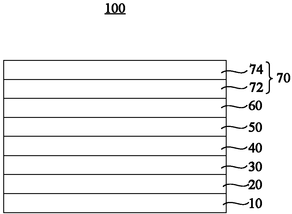
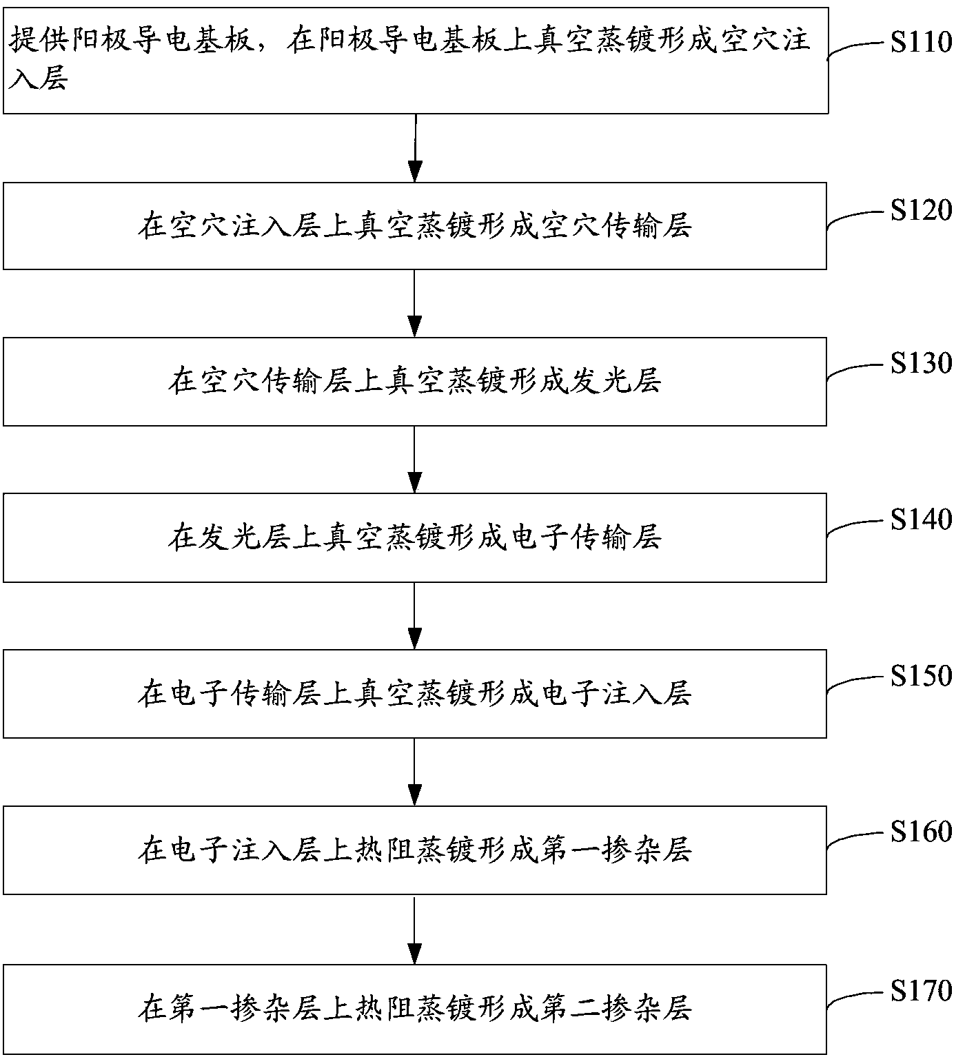
[0059] see figure 2 , a method for preparing an organic electroluminescent device according to one embodiment, comprising the following steps.
[0060] Step S110: providing an anode conductive substrate, and forming a hole injection layer by vacuum evaporation on the anode conductive substrate.
[0061] The anode conductive substrate 10 is a glass substrate with conductive patterns laminated on its surface, preferably indium tin oxide glass substrate (ITO), aluminum zinc oxide glass substrate (AZO) or indium zinc oxide glass substrate (IZO).
[0062] The glass substrate laminated with the conductive thin film is subjected to photolithography treatment, and cut into the required size to obtain the glass substrate laminated with the conductive pattern, that is, the anode conductive substrate. The conductive film is an ITO film, AZO film or IZO film.
[0063] The hole injection layer is formed by vacuum evaporation on the anode conductive substrate, and the working voltage is ...
Embodiment 1
[0096] The structure is ITO / MoO 3 / TCTA / Alq 3 / TAZ / LiF / P71BM:ReO 3 Preparation of Organic Electroluminescent Devices Based on / Ca:Ag:PO15
[0097] (1) To provide an anode conductive substrate, first, the glass laminated with indium tin oxide film is photolithographically processed, and cut into the required size to obtain the glass laminated with ITO conductive patterns, that is, the anode conductive substrate, expressed as ITO. Ultrasonic wash the anode conductive substrate with detergent and deionized water for 15 minutes in sequence to remove organic pollutants on the surface of the anode conductive substrate, dry and set aside;
[0098] (2) The hole injection layer is formed by vacuum evaporation on the anode conductive substrate, and the working pressure is 8×10 -5 Pa, the rate of vacuum evaporation is 0.2nm / s, the material of the hole injection layer is molybdenum trioxide, and the hole injection layer is expressed as MoO 3 , the thickness of the hole injection layer...
Embodiment 2
[0107] The structure is AZO / V 2 o 5 / TCTA / ADN / TAZ / CsF / C60:ReO 2 / Mg:Au:TAZ Fabrication of Organic Electroluminescent Devices
[0108] (1) To provide an anode conductive substrate, first, the glass laminated with aluminum zinc oxide film is photolithographically processed, and cut into the required size to obtain the glass laminated with AZO conductive patterns, that is, the anode conductive substrate, expressed as AZO. Ultrasonic wash the anode conductive substrate with detergent and deionized water for 15 minutes in sequence to remove organic pollutants on the surface of the anode conductive substrate, dry and set aside;
[0109] (2) The hole injection layer is formed by vacuum evaporation on the anode conductive substrate, and the working pressure is 2×10 -3 Pa, the rate of vacuum evaporation is 0.1nm / s, the material of the hole injection layer is vanadium pentoxide, and the hole injection layer is expressed as V 2 o 5 , the thickness of the hole injection layer is 80 n...
PUM
| Property | Measurement | Unit |
|---|---|---|
| Thickness | aaaaa | aaaaa |
| Thickness | aaaaa | aaaaa |
| Thickness | aaaaa | aaaaa |
Abstract
Description
Claims
Application Information
 - R&D
- Intellectual Property
- Life Sciences
- Materials
- Tech Scout
- Unparalleled Data Quality
- Higher Quality Content
- 60% Fewer Hallucinations
Browse by: Latest US Patents, China's latest patents, Technical Efficacy Thesaurus, Application Domain, Technology Topic, Popular Technical Reports.
© 2025 PatSnap. All rights reserved.Legal|Privacy policy|Modern Slavery Act Transparency Statement|Sitemap|About US| Contact US: help@patsnap.com