Floating gate flash memory device and programming method thereof

A technology of flash memory devices and programming methods, which is applied in the manufacture of electric solid-state devices, semiconductor devices, semiconductor/solid-state devices, etc., can solve the problems of high current power consumption and low efficiency of channel hot electron injection, etc., and achieve the reduction of current power consumption, Effect of suppressing short channel effect and improving coding efficiency

Active Publication Date: 2015-02-25
SHANGHAI HUALI MICROELECTRONICS CORP
View PDF6 Cites 3 Cited by
  • Summary
  • Abstract
  • Description
  • Claims
  • Application Information

AI Technical Summary

Problems solved by technology

[0005] However, the flash memory device disclosed in the above-mentioned patent has the following problems: in order to ensure high channel hot electron generation rate and high hot electron injection efficiency, a high voltage is applied to the drain and gate, and electrons flow from the source to the drain and Hot electrons are accelerated under the action of a high electric field near the drain, and part of the hot electrons pass through the oxide layer under the floating gate and enter the floating gate to complete the programming operation
Since the lateral electric field decreases with the increase of the gate voltage, and the vertical electric field increases with the increase of the gate voltage, a high voltage must be applied to both the drain and the gate, which brings about a decrease in the channel hot electron injection efficiency. The problem of low power consumption and high current consumption

Method used


Image

  • Floating gate flash memory device and programming method thereof
  • Floating gate flash memory device and programming method thereof

Examples


Embodiment 1

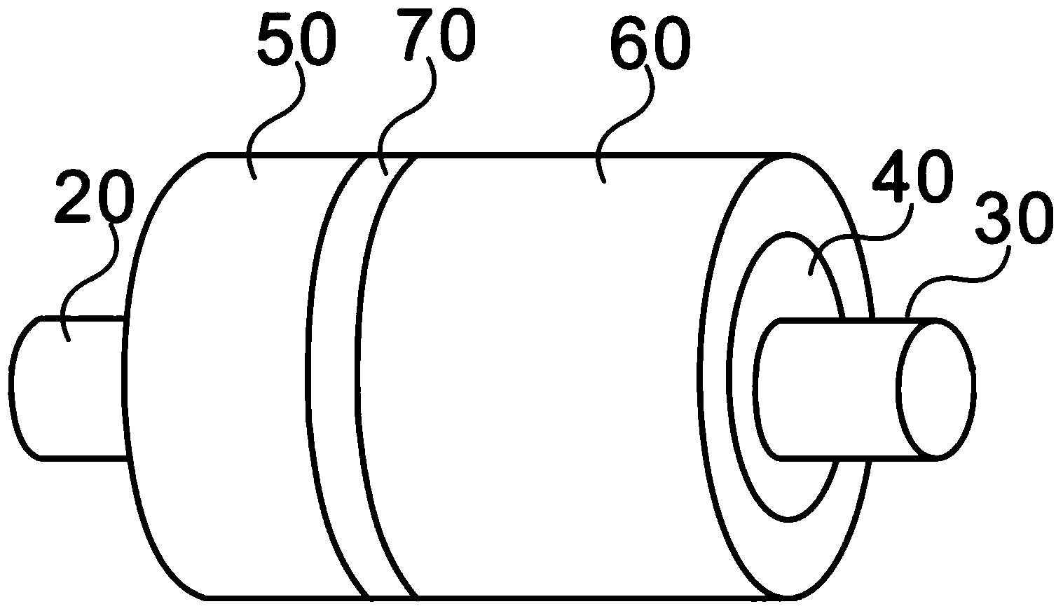
[0027] In this implementation, the control gate 50 and the floating gate 60 are made of polysilicon, the control gate 50 has a length of 10nm and a height of 90nm, and the floating gate 60 has a height of 70nm and a length of 40nm; the gate oxide layer 40 and the insulating layer 70 are made of silicon dioxide. The thickness of the gate oxide layer 40 is 2.5 nm, and the length of the insulating layer 70 is 3 nm. The manufacturing process of the device can be selected from the top-down technology compatible with the standard CMOS process.

[0028] The flash memory memory provided by the present invention adopts a cylindrical substrate structure on which the gate is covered. Compared with the prior art, the use of the cylindrical structure can enable the voltage of the control gate and the floating gate to better control the channel channel, suppress the short channel effect, resist the threshold voltage drift, and reduce the readout error of the flash memory.

[0029] The pres...

Embodiment 2

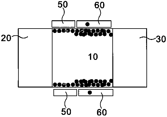
[0031] The voltage applied to the control gate 50 is equal to the threshold voltage of the flash memory device, the voltage applied to the floating gate 60 is twice the threshold voltage of the flash memory device, the voltage applied to the drain terminal 30 is 4V, and the voltage applied to the source terminal 20 is 0V.

[0032] The compiling principle of the present invention is: the voltage value applied by the control gate 50 is equal to the threshold voltage value of the flash memory device, and a thinner channel electron layer is induced in the lower substrate region; the voltage value applied by the floating gate 60 is the threshold value of the flash memory device Twice the voltage value, a thicker channel electron layer is induced in the lower channel electron layer; the voltage applied to the drain is 4V, which accelerates the electrons induced under the control gate, generates hot electrons with sufficient energy and passes through the floating gate The high voltage...


PUM


Abstract

The invention provides a floating gate flash memory device and a programming method of the floating gate flash memory device. The floating gate flash memory device comprise a substrate of a cylindrical structure, and a source end and a drain end are arranged at the two ends of the substrate; the middle of the substrate is covered with a grid, a gate oxide layer is arranged between the grid and the substrate, and the grid comprises a control gate and a floating gate. According to the programming method of the floating gate flash memory device, movement of hot electrons is assisted by applying bias voltage to provide sufficient energy to cross the gate oxide layer to complete compiling, the compiling efficiency of the flash memory is improved, and power consumption of compiling current is reduced; in addition, the floating gate flash memory device and the programming method of the floating gate flash memory device can effectively reduce the key size of the floating gate flash memory of a parse gate, increase the cell density of a flash memory array and namely increases the storage capacity and density of the flash memory.

Description

technical field [0001] The invention relates to the field of semiconductor integrated circuits and its manufacture, in particular to a floating gate flash memory device and a programming method thereof. Background technique [0002] In semiconductor storage devices, flash memory is a non-volatile memory, and belongs to erasable programmable read-only memory (EPROM). Generally, a flash memory has two gates (a floating gate and a control gate), wherein the floating gate is used to store charges, and the control gate is used to control data input and output. The position of the floating gate is below the control gate, and it is in a floating state because it is not connected to the external circuit. The advantage of flash memory is that it can erase the entire memory block, and the erasing speed is fast, only about 1 to 2 seconds. Generally speaking, flash memory has a split gate structure or a stacked gate structure or a combination of the two structures. Due to its special...

Claims


Application Information

Patent Timeline
Patent Type & Authority Applications(China)
IPC IPC(8): H01L29/788H01L27/115H01L21/8247
CPCH10B41/00
Inventor 顾经纶
Owner SHANGHAI HUALI MICROELECTRONICS CORP
Why Eureka
Try Eureka