A Laser Powder Deposition Method for Controlling the Interface Morphology of Thermal Barrier Coatings
A technology of laser powder and thermal barrier coating, which is applied in the direction of coating, superimposed layer plating, metal material coating process, etc., which can solve the problem of interface toughness decline, ceramic layer peeling, interface bonding strength, and crack growth inhibition. and other problems, to achieve the effect of enhancing the mechanical bonding strength and increasing the service life of the thermal cycle
- Summary
- Abstract
- Description
- Claims
- Application Information
AI Technical Summary
Problems solved by technology
Method used
Image
Examples
Embodiment 1
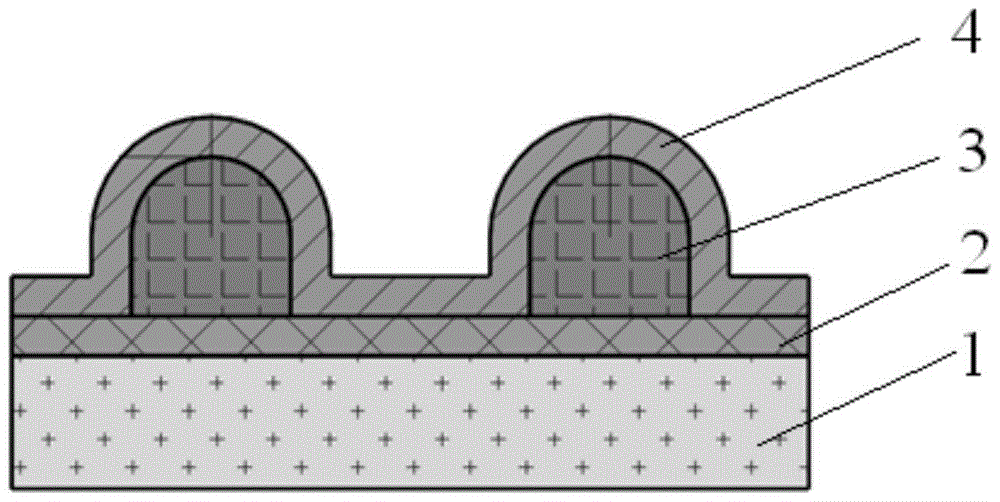
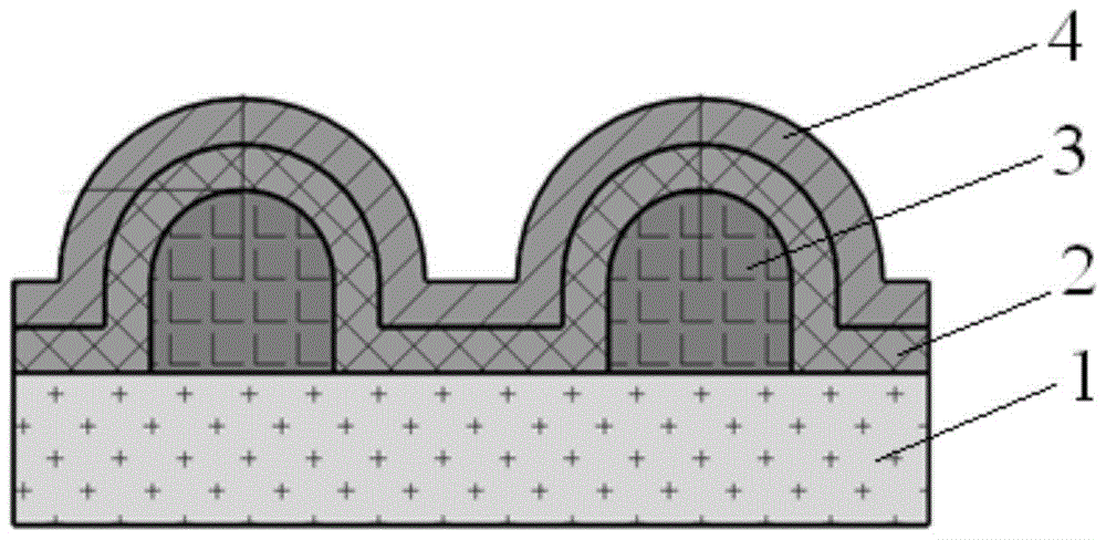
[0031] First, the Hastelloy superalloy substrate is cleaned, degreased and sandblasted, and then a NiCrAlY metal bonding layer with a thickness of 150 μm is deposited on the substrate by atmospheric plasma spraying. According to the set parameters, laser powder deposition technology is used to introduce a grid layer on its surface such as figure 2 As shown, the spacing between the grids is 2.5 mm, the height is 500 μm, the width of a single metal grid is 500 μm, the composition is the same as that of the bonding layer, and the upper surface of the grid is an arc surface. The maximum power of the fiber laser is 1000W, the spot diameter of the laser beam is 600μm, the laser power is 80-120W, and the flow rate is 6L / min. min. Finally a ceramic layer with a thickness of 200 μm was deposited by atmospheric plasma spraying. After a thermal cycle at 1150°C, the thermal barrier coating (without grid structure) of the traditional structure has a peeling area of more than 50%, whil...
Embodiment 2
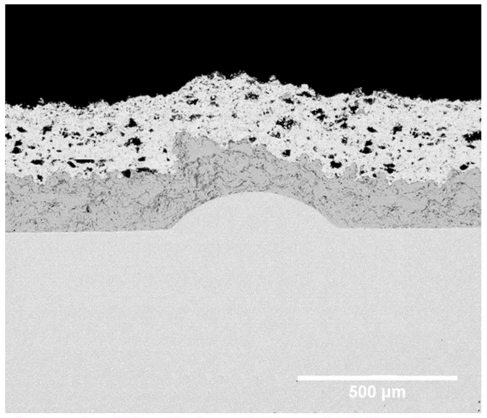
[0033]First, according to the conventional process, the Hastelloy superalloy substrate is cleaned, degreased, and sandblasted with alumina particles of a certain particle size. According to the experimental settings, the grid layer is introduced on the substrate by laser powder deposition technology. The specific parameters are: the grid spacing is 2.5 mm, the height is 130 mm, the single grid width is 500 μm, and the composition is Inconel718. The maximum power of the laser is 1000W, the beam spot diameter of the electron beam is 600μm, and the molten pool is protected by argon gas, the flow rate is 6L / min, and the powder feeding amount is 3g / min. Metallic bonding layers and ceramic layers with a thickness of 150 μm and 200 μm were then deposited thereon by atmospheric plasma spraying. The composition of the bonding layer is NiCrAlY, and the ceramic layer is 8YSZ. After a high-temperature thermal cycle at 1150°C, when the peeling area of the thermal barrier coating (withou...
PUM
| Property | Measurement | Unit |
|---|---|---|
| diameter | aaaaa | aaaaa |
| thickness | aaaaa | aaaaa |
| width | aaaaa | aaaaa |
Abstract
Description
Claims
Application Information
 - R&D
- Intellectual Property
- Life Sciences
- Materials
- Tech Scout
- Unparalleled Data Quality
- Higher Quality Content
- 60% Fewer Hallucinations
Browse by: Latest US Patents, China's latest patents, Technical Efficacy Thesaurus, Application Domain, Technology Topic, Popular Technical Reports.
© 2025 PatSnap. All rights reserved.Legal|Privacy policy|Modern Slavery Act Transparency Statement|Sitemap|About US| Contact US: help@patsnap.com


