Organic light emitting diode device and preparation method thereof
An electroluminescent device and a luminescent technology, which are applied in the direction of electric solid-state devices, semiconductor/solid-state device manufacturing, electrical components, etc., to achieve the effects of prolonging the life of the device, good buffering effect, and small internal stress
- Summary
- Abstract
- Description
- Claims
- Application Information
AI Technical Summary
Problems solved by technology
Method used
Image

Examples
Embodiment 1
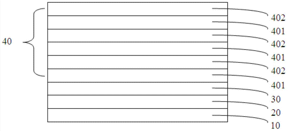
[0050] Such as figure 1 The schematic diagram of the structure of the organic electroluminescent device is shown. This embodiment provides a method for preparing an organic electroluminescent device, which includes the following steps:
[0051] (1) Prepare the light-emitting functional layer 20 and the cathode layer 30 on the anode substrate
[0052] a. Pretreatment of conductive glass substrate
[0053] Take the ITO glass substrate 10, and perform acetone cleaning→ethanol cleaning→deionized water cleaning→ethanol cleaning in sequence, all cleaning with an ultrasonic cleaning machine, washing and cleaning for 5 minutes, then blowing dry with nitrogen, and drying in an oven for later use; The cleaned ITO glass also needs surface activation treatment to increase the oxygen content of the conductive surface layer and improve the work function of the conductive layer surface; the thickness of ITO is 100nm;
[0054] b. Preparation of luminescent functional layer 20 and cathode la...
Embodiment 2
[0071] A method for preparing an organic electroluminescent device, comprising the following steps:
[0072] (1) Prepare the luminescent functional layer and the cathode layer on the anode substrate as in Example 1;
[0073] (2) Prepare the encapsulation layer on the cathode layer
[0074] a. Fabrication of germanium carbonitride barrier layer:
[0075] Depositing a germanium carbonitride barrier layer on the surface of the cathode layer by plasma enhanced chemical vapor deposition (PECVD), the material of the germanium carbonitride barrier layer is germanium carbonitride, and the deposited germanium carbonitride barrier layer The thickness is 140nm. In the process of depositing the germanium carbonitride barrier layer, the deposition temperature is 40°C, and the gas sources used are methylgermane (MMG), ammonia (NH 3) and hydrogen (H 2 ), wherein the flow rate of the MMG is 8sccm, the NH 3 / MMG ratio is 24, the H 2 The flow rate is 205sccm;
[0076] b. Fabrication of in...
Embodiment 3
[0081] A method for preparing an organic electroluminescent device, comprising the following steps:
[0082] (1) Preparation of luminescent functional layer and cathode layer on the anode substrate
[0083] With embodiment one;
[0084] (2) Prepare the encapsulation layer on the cathode layer
[0085] a. Fabrication of germanium carbonitride barrier layer:
[0086] Depositing a germanium carbonitride barrier layer on the surface of the cathode layer by plasma enhanced chemical vapor deposition (PECVD), the material of the germanium carbonitride barrier layer is germanium carbonitride, and the deposited germanium carbonitride barrier layer The thickness is 140nm. In the process of depositing the germanium carbonitride barrier layer, the deposition temperature is 50°C, and the gas sources used are methylgermane (MMG), ammonia (NH 3 ) and hydrogen (H 2 ), wherein the flow rate of the MMG is 6sccm, the NH 3 / MMG ratio is 21, the H 2 The flow rate is 210sccm;
[0087] b. Fab...
PUM
 Abstract
Description
Claims
Application Information
 - R&D
- Intellectual Property
- Life Sciences
- Materials
- Tech Scout
- Unparalleled Data Quality
- Higher Quality Content
- 60% Fewer Hallucinations
Browse by: Latest US Patents, China's latest patents, Technical Efficacy Thesaurus, Application Domain, Technology Topic, Popular Technical Reports.
© 2025 PatSnap. All rights reserved.Legal|Privacy policy|Modern Slavery Act Transparency Statement|Sitemap|About US| Contact US: help@patsnap.com