Organic light-emitting device packaging structure and packaging method thereof
A technology of electroluminescent devices and packaging structures, which is applied in organic light-emitting device structures, organic light-emitting devices, organic semiconductor devices, etc., and can solve the problem that the barrier performance of plastic substrates cannot meet the requirements of OLED packaging, and the life of flexible organic electroluminescent devices is short , There are many defects in the film structure of the device, etc., to achieve excellent packaging effect, benefit the life of the device, and reduce the effect of erosion
- Summary
- Abstract
- Description
- Claims
- Application Information
AI Technical Summary
Problems solved by technology
Method used
Image

Examples
Embodiment 1
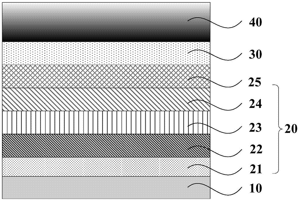
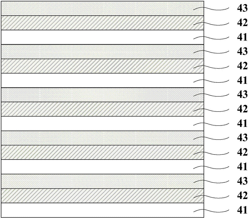
[0040] figure 1 It is a schematic diagram of the packaging structure of an organic electroluminescent device provided in this embodiment. Such as figure 1 As shown, the packaging structure of the organic electroluminescent device is sequentially stacked with a conductive glass substrate 10 , an organic light-emitting functional layer 20 , a metal cathode 30 and a packaging layer 40 . Wherein, the organic light-emitting functional layer 20 includes a hole injection layer 21 , a hole transport layer 22 , a light-emitting layer 23 , an electron transport layer 24 and an electron injection layer 25 stacked sequentially from bottom to top. figure 2 yes figure 1 Schematic diagram of the component structure of the encapsulation layer, such as figure 2 As shown, the encapsulation layer 40 includes a germanium oxycarbide layer 41 , a first barrier layer 42 and a second barrier layer 43 sequentially stacked on the metal cathode 30 . More specifically, the encapsulation layer 40 in...
Embodiment 2
[0056] A packaging structure of an organic electroluminescence device, which sequentially includes a conductive glass substrate, a hole injection layer, a hole transport layer, a light emitting layer, an electron transport layer, an electron injection layer, a metal cathode and a packaging layer from bottom to top. The encapsulation layer is made of 4 layers of germanium oxycarbide / Al 2 o 3 :Cl layer / ZrO 2 : Multilayer composite film structure composed of Cl layer. Its preparation method is as follows:
[0057] (1) Pre-treatment of ITO glass substrates: ITO glass substrates are cleaned with acetone, ethanol, deionized water, and ethanol, all of which are cleaned with an ultrasonic cleaner. The single washing is cleaned for 5 minutes, then blown dry with nitrogen, and dried in an oven Standby; the cleaned ITO glass also needs surface activation treatment to increase the oxygen content of the conductive surface layer and improve the work function of the conductive layer surfa...
Embodiment 3
[0071] A packaging structure of an organic electroluminescent device, which sequentially includes a conductive glass substrate, a hole injection layer, a hole transport layer, a light emitting layer, an electron transport layer, an electron injection layer, a metal cathode and a packaging layer from bottom to top. The encapsulation layer is composed of 3 layers of germanium oxycarbide / Ga 2 o 3 :Cl layer / HfO 2 : Multilayer composite film structure composed of Cl layer. Its preparation method is as follows:
[0072] (1) Pre-treatment of ITO glass substrates: ITO glass substrates are cleaned with acetone, ethanol, deionized water, and ethanol, all of which are cleaned with an ultrasonic cleaner. The single washing is cleaned for 5 minutes, then blown dry with nitrogen, and dried in an oven Standby; the cleaned ITO glass also needs surface activation treatment to increase the oxygen content of the conductive surface layer and improve the work function of the conductive layer su...
PUM
| Property | Measurement | Unit |
|---|---|---|
| Thickness | aaaaa | aaaaa |
| Thickness | aaaaa | aaaaa |
| Deposition thickness | aaaaa | aaaaa |
Abstract
Description
Claims
Application Information
 - Generate Ideas
- Intellectual Property
- Life Sciences
- Materials
- Tech Scout
- Unparalleled Data Quality
- Higher Quality Content
- 60% Fewer Hallucinations
Browse by: Latest US Patents, China's latest patents, Technical Efficacy Thesaurus, Application Domain, Technology Topic, Popular Technical Reports.
© 2025 PatSnap. All rights reserved.Legal|Privacy policy|Modern Slavery Act Transparency Statement|Sitemap|About US| Contact US: help@patsnap.com