Nitride LED epitaxial wafer structure based on copper substrate and manufacturing method thereof

A technology of LED epitaxial wafer and nitride epitaxial layer, which is applied to electrical components, circuits, semiconductor devices, etc., can solve the problems of expensive equipment, low process yield, complicated process, etc., and achieve the effect of cost saving

Inactive Publication Date: 2015-04-22
江苏巨晶新材料科技有限公司
View PDF4 Cites 35 Cited by
  • Summary
  • Abstract
  • Description
  • Claims
  • Application Information

AI Technical Summary

Problems solved by technology

Vertical chips represented by thin-film chips usually use laser lift-off to separate the sapphire substrate and epitaxial layer, but this method is complex in process, expensive in equipment, and low in process yield

Method used


Image

  • Nitride LED epitaxial wafer structure based on copper substrate and manufacturing method thereof
  • Nitride LED epitaxial wafer structure based on copper substrate and manufacturing method thereof
  • Nitride LED epitaxial wafer structure based on copper substrate and manufacturing method thereof

Examples


preparation example Construction

[0068] A method for preparing a nitride LED epitaxial wafer structure based on a copper substrate, comprising the following steps:

[0069] 1) Prepare one or more two-dimensional derived film layers on a copper substrate to obtain a copper substrate with a two-dimensional derived film layer; specifically include three preparation methods:

[0070] Preparation method 1, directly using chemical vapor deposition on the copper substrate to prepare one or more graphene layers or hexagonal boron nitride layers;

[0071] The specific steps for preparing the graphene layer are as follows: the copper substrate is placed in a chemical vapor deposition system, and at a temperature of 400-1050 ° C, argon and hydrocarbons are simultaneously introduced to form a graphene layer on the copper substrate. graphene layer;

[0072] The specific steps for preparing hexagonal boron nitride are as follows: put the copper substrate into a chemical vapor deposition system, and at a temperature of 400...

Embodiment 1

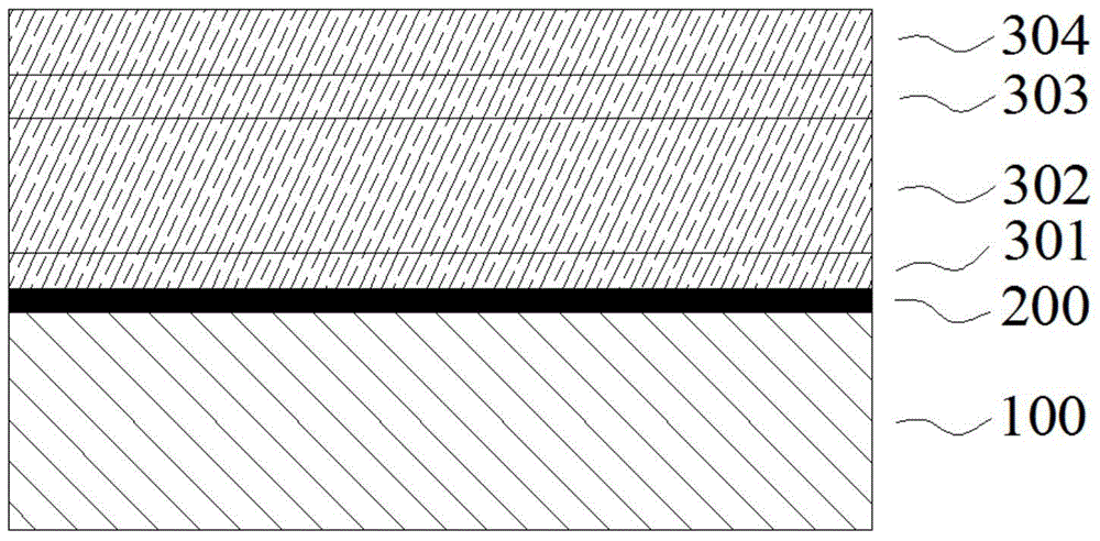
[0088] like figure 1 As shown, on top of a 2-inch, 80 μm thick copper substrate wafer 100, a single layer of graphene 201 is used as a two-dimensional derived film, and on the two-dimensional derived film is a nitride blue LED epitaxial layer. Wherein, the buffer layer 301 is made of 200nm n-type Al 0.1 Ga 0.9 N-layer composition; the structural parameters of the n-type electron injection layer 302 are as follows: a 2 μm thick n-type GaN layer, the doping element is Si, and the doping concentration is 1.0×10 19 ; The structural parameters of the active layer 303 are as follows: In 0.15 Ga 0.85 N / GaN multiple quantum well light-emitting layer, In 0.15 Ga 0.85 The single-layer thicknesses of N and GaN are 3nm and 10nm respectively, and the number of periods of the multiple quantum wells is 5; the structural parameters of the p-type hole injection layer 304 are as follows: it includes two sublayers, one is a 0.2 μm thick p-type GaN layer, The p-type doping element is Mg, an...

Embodiment 2

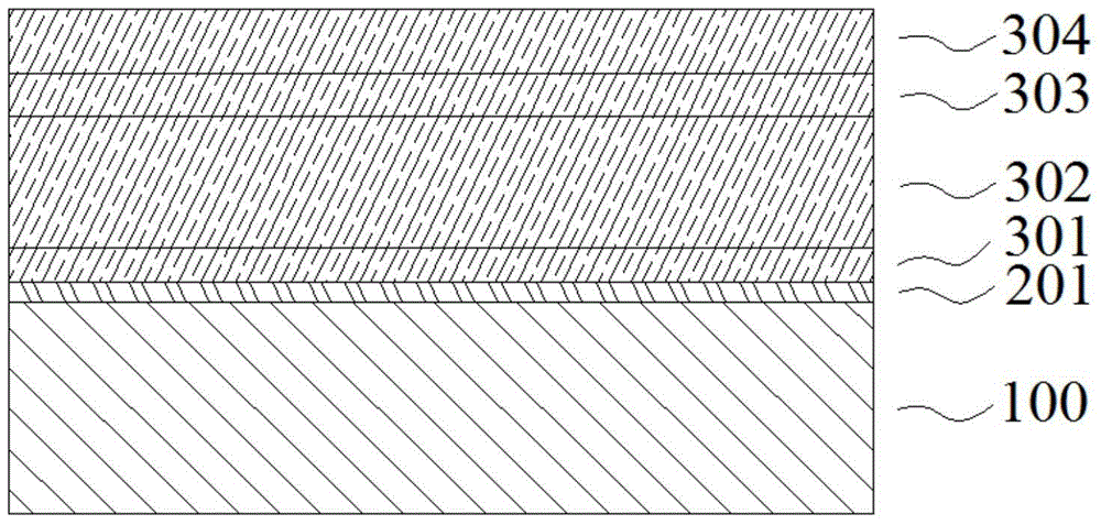
[0093] like image 3 As shown, on top of a 4-inch, 200 μm thick copper substrate wafer 100, a multi-layer hexagonal boron nitride (h-BN) 202 is used as a two-dimensional derived film, and a nitride blue LED is placed on the two-dimensional derived film epitaxial layer. Among them, the buffer layer 301 is made of 150nm n-type Al 0.3 Ga 0.7 N-layer structure; the structural parameters of the n-type electron injection layer 302 are as follows: a 2.5 μm thick n-type GaN layer, the doping element is Si, and the doping concentration is 1.5×10 19 ; The structural parameters of the active layer 303 are as follows: In 0.15 Ga 0.85 N / GaN multiple quantum well light-emitting layer, In 0.15 Ga 0.85 The single-layer thicknesses of N and GaN are 3nm and 10nm respectively, and the number of periods of the multiple quantum wells is 5; the structural parameters of the p-type hole injection layer 304 are as follows: it includes two sublayers, one is a 0.2 μm thick p-type GaN layer, The p...


PUM

PropertyMeasurementUnit
thicknessaaaaaaaaaa
thicknessaaaaaaaaaa
thicknessaaaaaaaaaa

Abstract

The invention relates to a nitride LED epitaxial wafer structure based on a copper substrate and a manufacturing method of the nitride LED epitaxial wafer structure. The nitride LED epitaxial wafer structure based on the copper substrate comprises the copper substrate, a two-dimensional derived film and a nitride epitaxial layer. The two-dimensional derived film is located between the copper substrate and the nitride epitaxial layer and is attached to the surface of the copper substrate. The nitride epitaxial layer is attached to the two-dimensional derived film. The manufacturing method comprises the steps that one or two layers of two-dimensional derived films are manufactured on the copper substrate, and the nitride epitaxial layer is grown on the copper substrate with the two-dimensional derived films. By the adoption of the nitride LED epitaxial wafer structure based on the copper substrate, high-crystalline-quality nitride epitaxial growth can be conducted on the copper substrate, cost is reduced, and the optical property, the electrical property and the thermal property of a device are improved.

Description

technical field [0001] The invention relates to a nitride LED epitaxial wafer structure based on a copper substrate and a preparation method thereof, belonging to the technical field of manufacturing LED optoelectronic devices. Background technique [0002] Al nitride x In y Ga 1-x-y N (0≤x, y≤1; x+y≤1; wurtzite crystal structure) light-emitting diode LEDs made of semiconductor materials are gradually being used in electronic display screens, landscape lighting, miner's lamps, Widely used in street lamps, liquid crystal display backlight, general lighting, optical disk information storage, biomedicine and other fields. The above-mentioned compound semiconductors can cover the entire spectral energy range from infrared, visible to ultraviolet light, and the emission wavelength of LED devices can be accurately customized by controlling the cationic composition of the nitride alloy. From the perspective of the scope of application fields and market capacity, the application...

Claims


Application Information

Patent Timeline
Patent Type & Authority Applications(China)
IPC IPC(8): H01L33/32H01L33/12H01L33/00
CPCH01L33/0075H01L33/12H01L33/32H01L2933/0025
Inventor 马亮胡兵刘素娟李金权裴晓将
Owner 江苏巨晶新材料科技有限公司
Why Eureka
Try Eureka