Low temperature polycrystalline silicon film transistor and manufacturing method thereof

A technology of thin-film transistors and low-temperature polysilicon, which is applied in the direction of transistors, semiconductor/solid-state device manufacturing, semiconductor devices, etc., and can solve problems such as inability to control by region

Active Publication Date: 2015-04-29
CHENGDU VISTAR OPTEOLECTRONICS CO LTD
View PDF3 Cites 9 Cited by
  • Summary
  • Abstract
  • Description
  • Claims
  • Application Information

AI Technical Summary

Problems solved by technology

[0003] In the prior art, a layer of metal diffusion barrier layer, such as silicon dioxide, is usually deposited after the deposition of amorphous silicon, and then a layer of metal induction layer is sputtered to realize crystallization and contr

Method used


Image

  • Low temperature polycrystalline silicon film transistor and manufacturing method thereof
  • Low temperature polycrystalline silicon film transistor and manufacturing method thereof
  • Low temperature polycrystalline silicon film transistor and manufacturing method thereof

Examples


Embodiment Construction

[0024] The present invention will be further described below in conjunction with the accompanying drawings and specific embodiments, so that those skilled in the art can better understand the present invention and implement it, but the examples given are not intended to limit the present invention.

[0025] Such as Figures 1A to 1D A method of manufacturing a low-temperature polysilicon thin film transistor shown, the method comprising:

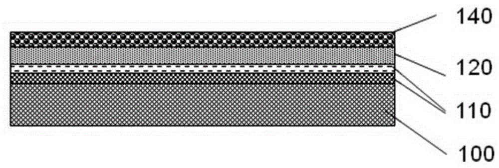
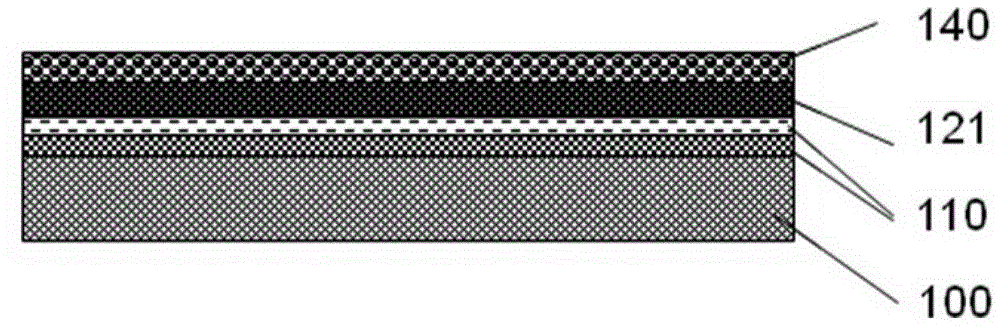
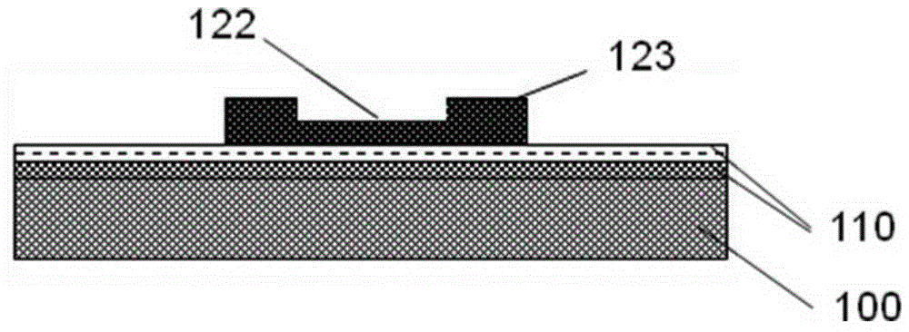
[0026] In step one, a buffer layer 110 is fabricated on the substrate 100 . The material of the substrate 100 can be glass, quartz, organic polymer, or opaque / reflective material, such as conductive material, wafer, ceramic, or other applicable materials. The buffer layer 110 may adopt a low pressure chemical vapor deposition process or an ion growth chemical vapor deposition process. In a specific embodiment, the buffer layer 110 may be a single layer or a double layer. The single-layer buffer layer 110 may be silicon oxide or silicon ni...


PUM


Abstract

The invention discloses a lower temperature polycrystalline silicon film transistor and a manufacturing method thereof. The method comprises the following steps: manufacturing a buffer layer on a substrate; manufacturing an amorphous silicon layer on the buffer layer; covering a metal induced layer on the amorphous silicon layer, and performing metal induced crystallization, so as to convert amorphous silicon layer into a polycrystalline silicon layer; schematizing the polycrystalline silicon layer to form a channel region and a source drain region; etching the surface layer, on which metallics remain due to metal induced crystallization, of the channel region; successively forming a gate-insulation layer, a gate, a layer insulation layer and a source drain electrode on the source drain region and the etched channel region. The polycrystalline silicon film transistor and the manufacturing method thereof, disclosed by the invention, realize the individual control of the density of the metallics on the channel region and the source drain region, so that not only is the density of the metallics on the channel region lower, but also the leaked current is reduced; the density of the metallics on the source drain region is higher, the metallics can be used as adulterants so as to reduce the technology of doping again, and besides, contact resistance is decreased; finally, the influence of the metallics remained in an active region on the performance of devices is eliminated.

Description

technical field [0001] The invention belongs to the technical field of semiconductors, and in particular relates to a low-temperature polysilicon thin film transistor and a manufacturing method thereof. Background technique [0002] Polysilicon material (poly-silicon, p-Si) has higher mobility compared with amorphous silicon material (a-Si). Therefore, using polysilicon to prepare thin film transistors can obtain devices with faster response. Generally speaking, a thin film transistor has at least a gate, a source, a drain, and an active layer. The conductivity of the active layer can be changed by controlling the voltage of the gate, so that a gap is formed between the source and the drain. In addition, an ohmic contact layer with N-type doping or P-type doping is usually formed on the active layer to reduce the contact between the active layer and the source, or The contact resistance between the channel layer and the drain. [0003] In the prior art, a layer of metal di...

Claims


Application Information

Patent Timeline
IPC IPC(8): H01L29/786H01L21/336
CPCH01L29/6675H01L29/78672
Inventor 齐之刚
Owner CHENGDU VISTAR OPTEOLECTRONICS CO LTD
Why Eureka
Try Eureka