
Composite channel MHEMT (Metamorphic High Electron Mobility Transistor) microwave oscillator and preparation method thereof

A microwave oscillator and composite channel technology, applied in the direction of electric solid-state devices, semiconductor devices, electrical components, etc., can solve the problems of limiting the development of HEMT devices on GaAs substrates, high manufacturing costs of InP substrates, and small dynamic range of devices. Achieve strong practicability and utilization value, enhance the concentration of two-dimensional electron gas and electron mobility, and achieve the effect of low phase noise

Active Publication Date: 2015-05-20
GUILIN UNIV OF ELECTRONIC TECH
View PDF7 Cites 13 Cited by
  • Summary
  • Abstract
  • Description
  • Claims
  • Application Information

AI Technical Summary

Problems solved by technology

However, the channel two-dimensional electron gas concentration and electron mobility of the traditional GaAs substrate HEMT are affected by the material structure and cannot make the conductive channel electron mobility and two-dimensional electron gas concentration very large, making the device work The small dynamic range limits the development of GaAs substrate HEMT devices in microwave oscillation circuits and microwave communications
Although the high electron mobility transistor channel of the InP substrate has a high two-dimensional electron gas concentration and electron mobility in the channel, the manufacturing cost of the InP substrate is high and the material is brittle, which is not conducive to popularization.

Method used


Image

  • Composite channel MHEMT (Metamorphic High Electron Mobility Transistor) microwave oscillator and preparation method thereof
  • Composite channel MHEMT (Metamorphic High Electron Mobility Transistor) microwave oscillator and preparation method thereof
  • Composite channel MHEMT (Metamorphic High Electron Mobility Transistor) microwave oscillator and preparation method thereof

Examples


Embodiment Construction

[0032] A preparation method of a composite channel MHEMT microwave oscillator, comprising the steps of:

[0033] Step 1: Epitaxial material growth.

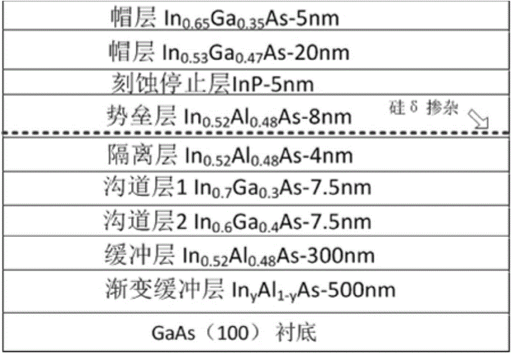
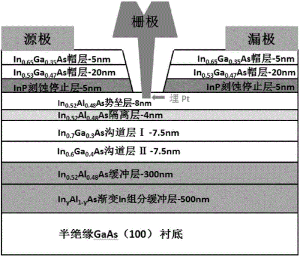
[0034] On the GaAs semi-insulating substrate layer, a 500nm variable In composition InAlAs buffer layer and a 300nm In 0.52 al 0.48 As buffer layer, 7.5nm In 0.6 Ga 0.4 As conductive channel layer, 7.5nm In 0.7 Ga 0.3 As conductive channel layer, 4nm In 0.52 al 0.48 As isolation layer, 8nm In 0.52 al 0.48 As barrier layer, 5nm InP etch stop layer, 20nm In 0.53 Ga 0.47 As cap layer, 5nm In 0.65 Ga 0.35 The As cap layer forms a GaAs substrate variable composition epitaxial material structure. see figure 1 It is a structural diagram of a composite channel GaAs substrate variable composition epitaxial material.

[0035] Step 2: device isolation is formed.

[0036]Uniform photolithography to protect the table. First, the surface of the sample was pretreated with HMDS in order to enhance the adhesion of the photoresist...


PUM


Abstract

The invention discloses a composite channel MHEMT (Metamorphic High Electron Mobility Transistor) microwave oscillator and a preparation method thereof. The device is of a composite channel structure; mesa isolation of combined ion injection and wet corrosion is adopted; a source-drain metallic system of Ni / AuGe / Ni / Au forms ohmic contact; a T-shaped gate is manufactured by using a three-layer resist technology of two self-alignment processes of an electronic exposure beam and one development process; two different kinds of corrosion solution are used for corroding to form a gate groove; a vaporized Pt / Ti / Pt / Au metallic system forms schottky contact in the gate groove; buried Pt is formed through annealing treatment; a silicon nitride passivation layer is formed; thus the preparation of the device is finished. The oscillator and the method have the advantages of simple process, high reliability of the device and convenience in repetition. Superior direct current performance and alternating current performance are obtained by using the prepared device with gate length of 80 nanometers, the maximum output saturation current reaches 920 mA / mm, and the extrinsic transconductance reaches 1,100 mS / mm. The characteristic frequency of the device reaches 246GHz, and the maximum oscillation frequency is 301GHz.

Description

technical field [0001] The invention belongs to the field of microwave communication devices, in particular to a composite channel MHEMT (variable composition high electron mobility transistor) microwave oscillator and a preparation method thereof. Background technique [0002] Microwave oscillators are very important components in microwave receiving systems. At present, there are two types of commonly used microwave oscillations, namely electric vacuum devices and solid state devices. Electric vacuum devices mainly include microwave electric vacuum triodes, reflection klystrons, magnetrons and return wave tubes; solid devices include crystal triodes, body effect diodes (also known as Gunn diodes) and avalanche diodes. Due to the relatively harsh requirements on the manufacturing environment and process of the electric vacuum device, its manufacturing cost is high, and it cannot be popularized and promoted, so it is rarely used in microwave mobile communication equipment. ...

Claims


Application Information

Patent Timeline
IPC IPC(8): H01L27/04
Inventor 李海鸥吉宪李琦李跃黄伟马磊首照宇吴笑峰李思敏
Owner GUILIN UNIV OF ELECTRONIC TECH
Learn More