Organic light-emitting device and preparation method thereof

An electroluminescent device and electroluminescent technology, which can be used in organic light-emitting devices, organic light-emitting device structures, organic semiconductor devices, etc., and can solve problems such as high cost, limited OLED product performance, and poor mechanical strength.

Inactive Publication Date: 2015-05-20
OCEANS KING LIGHTING SCI&TECH CO LTD +2
View PDF0 Cites 0 Cited by
  • Summary
  • Abstract
  • Description
  • Claims
  • Application Information

AI Technical Summary

Problems solved by technology

[0004] For OLED products, if the traditional OLED packaging technology is used, adding a packaging cover on the back of the device will cause problems such as heavy weight, high cost, and poor mechanical stren

Method used


Image

  • Organic light-emitting device and preparation method thereof
  • Organic light-emitting device and preparation method thereof
  • Organic light-emitting device and preparation method thereof

Examples


Embodiment 1

[0087] An organic electroluminescent device is prepared through the following steps:

[0088] (1) Provide a clean anode conductive substrate:

[0089] Clean the ITO glass substrate with acetone, ethanol, deionized water, and ethanol in an ultrasonic cleaner in sequence, wash and wash for 5 minutes in one item, then blow dry with nitrogen, and dry in an oven for later use; surface activation of the cleaned ITO glass processing; ITO thickness is 100nm;

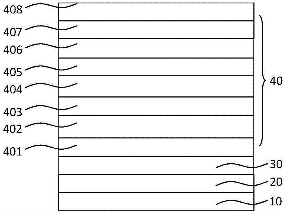
[0090] (2) Vacuum evaporation of the luminescent functional layer on the ITO glass substrate:

[0091] Specifically, the light emitting functional layer includes a hole injection layer, a hole transport layer, a light emitting layer, an electron transport layer and an electron injection layer;

[0092] Preparation of the hole injection layer: the MoO 3 The mixture obtained by mixing with NPB according to the mass ratio of 3:7 is used as the material of the hole injection layer, the thickness is 10nm, and the vacuum degree is ...

Embodiment 2

[0110] An organic electroluminescent device is prepared through the following steps:

[0111] (1), (2), (3) are the same as embodiment 1;

[0112] (4) Prepare the encapsulation layer on the outside of the cathode:

[0113] The encapsulation layer is an alternately stacked inorganic barrier layer and a mixed barrier layer;

[0114] Fabrication of the inorganic barrier layer: the organic electroluminescent device sample prepared with the cathode is placed in the deposition chamber of the atomic layer deposition system, and then,

[0115] (a) The metal source Mg(CpEt) 2 Inject nitrogen into the deposition chamber and deposit on the cathode, the injection time is 20ms, and the nitrogen flow rate is 20sccm;

[0116] (b) Inject nitrogen gas to flush the deposition chamber, the injection time is 10s, and the flow rate is 20 sccm;

[0117] (c) Water vapor is then injected into the deposition chamber along with nitrogen gas to react with the metal source. The injection time is 20 m...

Embodiment 3

[0123] An organic electroluminescent device is prepared through the following steps:

[0124] (1), (2), (3) are the same as embodiment 1;

[0125] (4) Prepare the encapsulation layer on the outside of the cathode:

[0126] The encapsulation layer is an alternately stacked inorganic barrier layer and a mixed barrier layer;

[0127] Fabrication of the inorganic barrier layer: the organic electroluminescent device sample prepared with the cathode is placed in the deposition chamber of the atomic layer deposition system, and then,

[0128] (a) The metal source Ca(CpEt) 2 Inject nitrogen into the deposition chamber and deposit on the cathode, the injection time is 10ms, and the nitrogen flow rate is 10sccm;

[0129] (b) Inject nitrogen gas to flush the deposition chamber, the injection time is 5s, and the flow rate is 10 sccm;

[0130] (c) Water vapor is then injected into the deposition chamber along with nitrogen gas to react with the metal source. The injection time is 10 ms...


PUM

PropertyMeasurementUnit
Thicknessaaaaaaaaaa
Thicknessaaaaaaaaaa
Thicknessaaaaaaaaaa

Abstract

The invention provides an organic light-emitting device with a packaging layer structure. The packaging layer structure is formed by alternate overlapping of inorganic barrier layers and mixed barrier layers. The inorganic barrier layers are made of one of BeO, MgO, CaO, SrO and BaO. Each mixed barrier layer is made of a mixture formed by one of AlF3, HfF4, ZrF4, LiF, CeF2 and YF3 and straight-chain gallane with a structural formula shown in the original text, wherein k refers to 1, 2, 3 or 4, and mole ratio of fluorides accounts for 20%-40%. The packaging layer structure is capable of effectively preventing external active materials such as water, oxide and the like from eroding the organic light-emitting device, so that the service life of the organic light-emitting device can be prolonged. The invention further provides a preparation method of the organic light-emitting device. The preparation method has the advantages of technical simplicity, low cost of raw materials and easiness for large-scale preparation.

Description

technical field [0001] The invention relates to the field of organic electroluminescence, in particular to an organic electroluminescence device and a preparation method thereof. Background technique [0002] An organic electroluminescent device (OLED) is an energy conversion device that uses organic materials as light-emitting materials and can convert applied electrical energy into light energy. It has outstanding performances such as ultra-thin, self-luminous, fast response, low power consumption, etc., and has extremely broad application prospects in display, lighting and other fields. [0003] Organic electroluminescent materials are particularly sensitive to oxygen and moisture intrusion. On the one hand, because oxygen is a quencher, the quantum efficiency of luminescence will be significantly reduced, and the oxidation of oxygen to the hole transport layer will also reduce its transport ability; on the other hand, water vapor will hydrolyze organic compounds, making...

Claims


Application Information

Patent Timeline
IPC IPC(8): H01L51/52H01L51/54H01L51/56
CPCH10K85/60H10K50/8445H10K50/84H10K2102/00H10K2102/302H10K71/00
Inventor 周明杰钟铁涛王平冯小明
Owner OCEANS KING LIGHTING SCI&TECH CO LTD
Why Eureka
Try Eureka