Longitudinal conduction GaN (gallium nitride) normally-off MISFET (metal-insulator-semiconductor field effect transistor) device and manufacturing method thereof

A normally-off, on-state technology, used in semiconductor/solid-state device manufacturing, semiconductor devices, electrical components, etc., can solve problems such as deteriorating the quality of the electron blocking layer, cleaning the mask layer, and degrading device performance. control capability, improved device performance, reduced on-resistance

Active Publication Date: 2015-06-03
SHANGHAI XINYUANJI SEMICON TECH
View PDF6 Cites 8 Cited by
  • Summary
  • Abstract
  • Description
  • Claims
  • Application Information

AI Technical Summary

Problems solved by technology

Selected area growth generally requires a patterned mask layer (commonly used such as SiO 2 ) to select the area to be grown, but this mask process will encounter the following problems: it is difficult to etch the mask layer when it is removed by etching, and there will be a large amount of impurities remaining on the secondary growth interface (such as Si ), in the secondary epitaxial growth, the residual impurity element is very easy to diffuse upward into the electron blocking layer under the high temperature growth environment, thereby compensating with the p-type doping element (commonly used such as Mg) of the electron blocking layer , which seriously deteriorates the quality of the electron blocking layer, resulting in a significant drop in device performance

Method used


Image

  • Longitudinal conduction GaN (gallium nitride) normally-off MISFET (metal-insulator-semiconductor field effect transistor) device and manufacturing method thereof
  • Longitudinal conduction GaN (gallium nitride) normally-off MISFET (metal-insulator-semiconductor field effect transistor) device and manufacturing method thereof
  • Longitudinal conduction GaN (gallium nitride) normally-off MISFET (metal-insulator-semiconductor field effect transistor) device and manufacturing method thereof

Examples


Embodiment 1

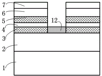
[0039] Such as Figure 9 Shown is a schematic diagram of the device structure of this embodiment, the device includes a gate, a source, a drain, an insulating layer, a conductive GaN substrate and an epitaxial layer thereon, and the epitaxial layer includes an n-type lightly doped A doped GaN layer and a secondary epitaxial layer grown on it in a selective region, the secondary epitaxial layer is an impurity filter layer 1, an electron blocking layer, an impurity filter layer 2, a non-doped epitaxial GaN layer and a heterostructure from bottom to top The barrier layer, the groove channel is formed after the second epitaxial growth, the surface of the groove channel and the heterostructure barrier layer is covered with an insulating layer, the gate is covered with the groove channel on the insulating layer, and the insulating layer is etched A source region is formed at both ends, and ohmic metal is evaporated on the source region to form a source in contact with the heterojunc...

Embodiment 2

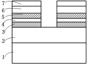
[0052] Such as Figure 10 Shown is a schematic diagram of the device structure of this embodiment, which is similar to the structure of Embodiment 1, the only difference being that an n-type heavily doped GaN layer 13 with a thickness of 10-100 nm is inserted on the n-type lightly doped GaN layer 2 . The n-type heavily doped GaN layer 13 is in direct contact with the gate channel, which can effectively diffuse the gate channel current and disperse the concentrated electric field near the gate, thereby increasing the maximum breakdown voltage of the device.

Embodiment 3

[0054] Such as Figure 11 Shown is a schematic diagram of the device structure of this embodiment, which is similar to the structure of Embodiment 1, the only difference is that an AlN layer 14 is inserted between the non-doped GaN layer 6 and the heterostructure barrier layer 7, and the AlN layer can improve heterogeneity. 2DEG mobility in the channel of the matrix structure.


PUM


Abstract

The invention relates to a longitudinal conduction GaN (gallium nitride) normally-off MISFET (metal-insulator-semiconductor field effect transistor) device and a manufacturing method of the MISFET device, wherein an epitaxial layer comprises a primary epitaxial growth n type light-doped GaN layer and a secondary epitaxial layer growing in a selection area of the light-doped GaN layer; the secondary epitaxial layer comprises a first impurity filtering layer, an electron blocking layer, a second impurity filtering layer, a non-doped epitaxial GaN layer and a heterostructure barrier layer from bottom to top; a groove channel is formed after secondary epitaxial growth; an insulating layer covers the surface of the groove channel and the surface of the heterostructure barrier layer; a grid electrode covers the groove channel on the insulating layer; two source electrode areas are respectively formed at two ends of the insulating layer by etching; two pieces of ohmic metal are respectively arranged at the source electrode areas by evaporation, so that source electrodes contacted with the heterostructure barrier layer can be formed; a piece of drain electrode ohmic contact metal is arranged at the back of a conductive GaN substrate. The MISFET device is simple in structure and high in process repeatability and reliability, and is capable of effectively inhibiting the diffusion of impurities in a secondary growth interface or the electron blocking layer, so that the electrical properties of 2DEG of the electron blocking layer and a heterostructure channel can be optimized.

Description

technical field [0001] The present invention relates to the technical field of semiconductor devices, and more specifically, to a GaN normally-off MISFET device with vertical conduction and a manufacturing method thereof. Background technique [0002] GaN semiconductor materials have superior properties such as large band gap, high breakdown electric field, large saturated electron drift velocity and high thermal conductivity, and there is a two-dimensional electron gas (2DEG) with high concentration and high electron mobility at the heterojunction interface. Compared with Si materials, it is more suitable for the preparation of power electronic devices with high power, large capacity and high switching speed, and becomes an ideal substitute for the next generation of power switching devices. [0003] GaN power switching devices are divided into lateral conduction devices and vertical conduction devices from the perspective of device structure. The lateral conduction devic...

Claims


Application Information

Patent Timeline
Patent Type & Authority Applications(China)
IPC IPC(8): H01L29/78H01L29/06H01L21/336
CPCH01L29/0657H01L29/66477H01L29/7838
Inventor 刘扬何亮杨帆姚尧倪毅强
Owner SHANGHAI XINYUANJI SEMICON TECH
Why Eureka
Try Eureka