Waveguide coupling type separate absorption and multiplication avalanche diode

An avalanche diode and coupling type technology, applied in semiconductor devices, electrical components, circuits, etc., can solve the problems of inability to achieve high sensitivity and large bandwidth industrial integration, reduce transit time and dark current, avoid disturbance phenomenon, improve Effect of Optical Coupling Efficiency

Active Publication Date: 2015-06-03
江苏浦丹光电技术有限公司
View PDF3 Cites 15 Cited by
  • Summary
  • Abstract
  • Description
  • Claims
  • Application Information

AI Technical Summary

Problems solved by technology

However, the waveguide absorption multiplication separation type avalanche detectors currently researched are still unable to achieve industrial integration with high sensitivity and large bandwidth.

Method used


Image

  • Waveguide coupling type separate absorption and multiplication avalanche diode
  • Waveguide coupling type separate absorption and multiplication avalanche diode
  • Waveguide coupling type separate absorption and multiplication avalanche diode

Examples


Embodiment Construction

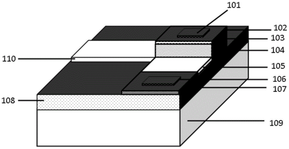
[0018] As shown in Figure 4, its preparation process and method are as follows:

[0019] 1. Etching the single-mode Si waveguide 110 and the Si region of the device on the top layer of 220 nm thick Si of a silicon-on-insulator (SOI) substrate.

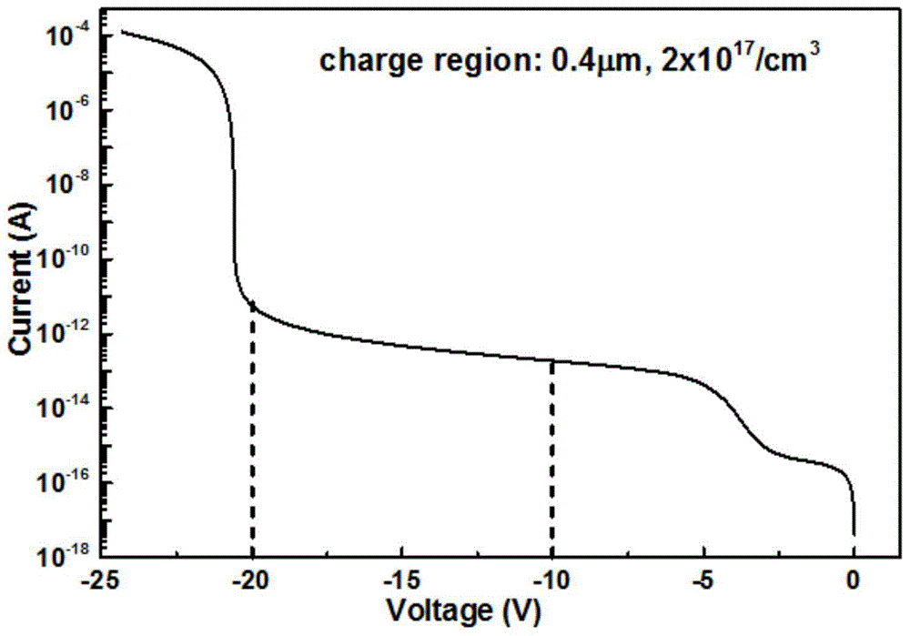
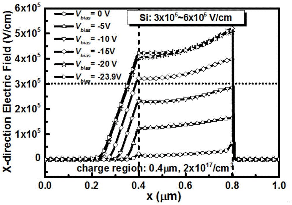
[0020] 2. Boron is implanted to form a p-type charge region 104 with a doping concentration of 2×10 17 cm -3 ;

[0021] 3. Deposit a layer of SiO on the surface 2 , a Ge epitaxial window is etched by a combination of dry and wet methods, and the intrinsic Ge layer is epitaxially selected, with a thickness of about 0.5 μm;

[0022] 4. Implant boron in the top layer of Ge region to form p + The ohmic contact layer 102 has a thickness of about 0.1 μm and a doping concentration of 1×10 19 cm -3 , and the remaining part is the Ge absorbing layer 103;

[0023] 5. Phosphorus ion implantation forms n + Ohmic contact region 107, the doping concentration is 1×10 19 cm -3 ;

[0024] 6. Rapid annealing to activate the implanted impurity...


PUM


Abstract

The invention discloses a waveguide coupling type separate absorption and multiplication avalanche diode, which relates to the field of semiconductor photoelectric devices and the field of optical interconnection. The waveguide coupling type separate absorption and multiplication avalanche diode comprises a p plus type ohmic contact electrode, a p plus type ohmic contact layer, an absorption layer, a p type charge region, a multiplication region, an n plus type ohmic contact electrode, an n plus type ohmic contact region, an insulated burial layer, a substrate and a single-mode waveguide; the waveguide coupling type separate absorption and multiplication avalanche diode is characterized that the p type charge region is positioned at the tail end of the single-mode waveguide, the absorption layer is positioned at the top part of the p type charge region, the multiplication region and the n plus type ohmic contact region are coplanar with the single-mode waveguide and are tightly close to the p type charge region to be sequentially arranged, stretching directions of the p type charge region, the multiplication region and the n plus type ohmic contact region are vertical to a light transmission direction of the single-mode waveguide, and the p type charge region, the multiplication region and the n plus type ohmic contact region are in the same thickness with the single-mode waveguide. According to the waveguide coupling type separate absorption and multiplication avalanche diode disclosed by the invention, the optical coupling efficiency is increased by a device by utilizing the coupling of the single-mode waveguide while the separate absorption and multiplication is realized, a disturbance phenomenon of electric signals of double multiplication regions is avoided, the size of the device can be reduced to nanometer size, the transition time and the dark current can be reduced, and the sensitivity is increased.

Description

technical field [0001] The invention relates to the field of semiconductor optoelectronic devices and the field of optical interconnection, in particular to a waveguide absorption multiplication separation type avalanche diode capable of detecting weak communication optical signals. Background technique [0002] Avalanche photodetector (APD) is an important branch of photodetector research that uses the avalanche multiplication effect to achieve photocurrent multiplication inside the device. The device has higher sensitivity and photoresponse, and is mainly used for the detection of weak light signals, especially The application of high-loss big data transmission technologies such as wavelength division multiplexing and time division multiplexing has made the sensitivity requirements of the optical receiving end higher and higher. Therefore, the avalanche photodetector is an important research direction in the field of optical communication and optical switching. [0003] A...

Claims


Application Information

Patent Timeline
Patent Type & Authority Applications(China)
IPC IPC(8): H01L29/861
Inventor 李冲郭霞刘巧莉董建刘白马云飞
Owner 江苏浦丹光电技术有限公司
Why Eureka
Try Eureka