Perovskite type electroluminescence device and preparation method thereof

An electroluminescent device, perovskite-type technology, applied in the direction of electric solid-state devices, semiconductor/solid-state device manufacturing, electrical components, etc., can solve the problems of low quantum efficiency, poor film quality of the light-emitting layer, high turn-on voltage, etc., to achieve The effect of reducing the electrode work function, good photoelectric performance, and low turn-on voltage

Active Publication Date: 2015-06-03
NANJING UNIV OF TECH
View PDF5 Cites 72 Cited by
  • Summary
  • Abstract
  • Description
  • Claims
  • Application Information

AI Technical Summary

Problems solved by technology

However, due to the limitations of the device structure and the poor film quality of the light-emitting layer, most current LEDs based on perovskite materials need to achieve light emission at low temperature conditions, high turn-on voltage, and low quantum efficiency (“Bright light- emitting diodes based on organometal halide perovskite”, Nat. Nanotechnol, 9, 687-692, 2014)

Method used


Image

  • Perovskite type electroluminescence device and preparation method thereof
  • Perovskite type electroluminescence device and preparation method thereof
  • Perovskite type electroluminescence device and preparation method thereof

Examples


Embodiment 1

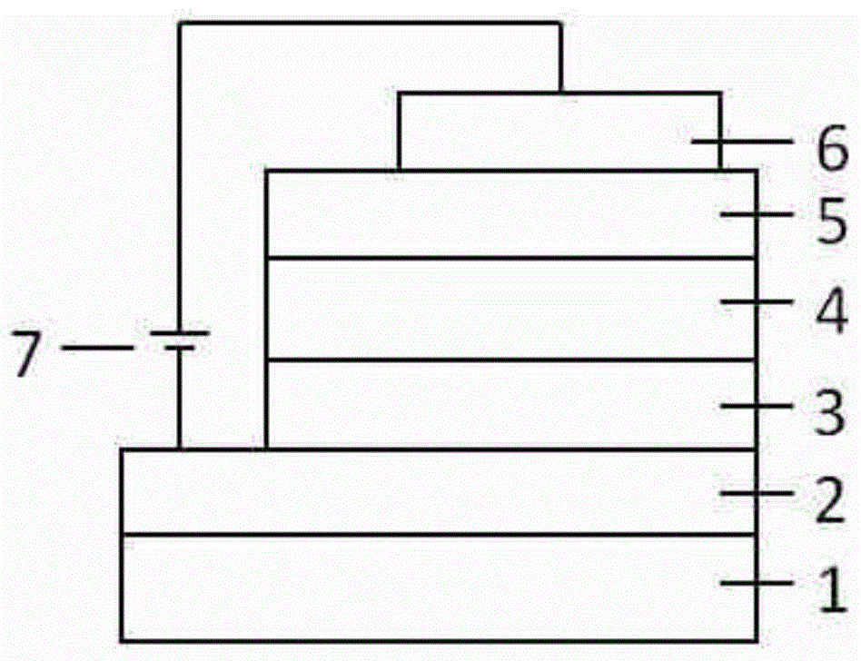
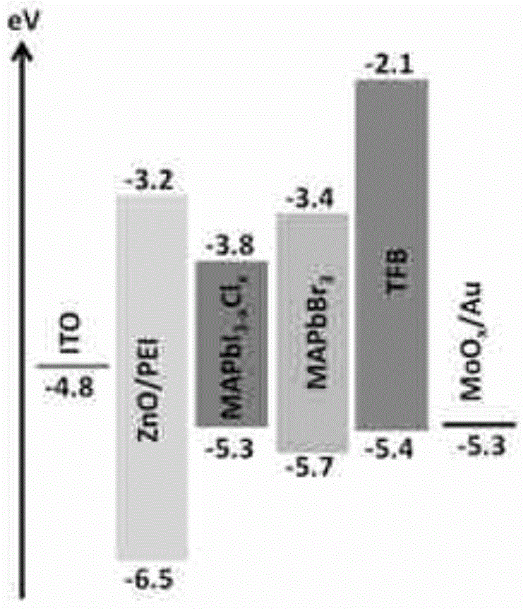
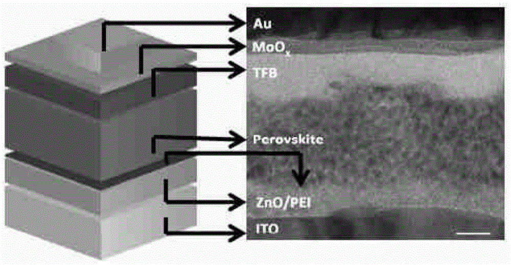
[0061] Such as image 3 As shown, the substrate is a glass-ITO combination, the electron transport-hole blocking layer is ZnO / PEI, and the light-emitting layer is CH 3 NH 3 PbBr 3 , hole transport-electron blocking layer is TFB, top electrode is MoO x / Au, the entire device structure is described as: glass substrate / ITO / ZnO-PEI(20nm) / CH 3 NH 3 PbBr 3 (50nm) / TFB(25nm) / MoO x (8nm) / Au(100nm).

[0062] The preparation method is as follows:

[0063] ①Use ethanol solution, acetone solution and deionized water to ultrasonically clean the transparent conductive substrate ITO glass, and dry it with dry nitrogen after cleaning. The ITO film on the glass substrate is used as the anode layer of the device, and the sheet resistance of the ITO film is 15Ω / □.

[0064] ② Move the dried substrate into a vacuum chamber, and pretreat the ITO glass with ultraviolet and ozone for 10 minutes under an oxygen pressure environment.

[0065] ③ Spin-coat ZnO and PEI on the treated substrate re...

Embodiment 2

[0073] On the basis of Example 1, the halogen elements of the perovskite material in the light-emitting layer are changed, and the perovskite material CH with narrow band gap and near-infrared light emission is used. 3 NH 3 PB 3-x Cl x , the substrate is a glass-ITO combination, the electron transport-hole blocking layer is ZnO / PEI, the hole transport-electron blocking layer is TFB, and the top electrode is MoO x / Au, the entire device structure is described as: glass substrate / ITO / ZnO-PEI(20nm) / CH 3 NH 3 PB 3-x Cl x (50nm) / TFB(25nm) / MoO x (8nm) / Au(100nm).

[0074] The preparation method is as follows:

[0075] ①Use ethanol solution, acetone solution and deionized water to ultrasonically clean the transparent conductive substrate ITO glass, and dry it with dry nitrogen after cleaning. The ITO film on the glass substrate is used as the anode layer of the device, and the sheet resistance of the ITO film is 15Ω / □.

[0076] ② Move the dried substrate into a vacuum chambe...

Embodiment 3

[0084] On the basis of Example 1, change the perovskite layer CH 3 NH 3 PbBr 3 The film-forming method, the light-emitting layer is prepared by two-step spin coating, the substrate is a glass-ITO combination, the electron transport-hole blocking layer is ZnO / PEI, the hole transport-electron blocking layer is TFB, and the top electrode is MoO x / Au, the entire device structure is described as:

[0085] Glass substrate / ITO / ZnO-PEI(20nm) / CH 3 NH 3 PbBr 3 (50nm) / TFB(25nm) / MoO x (8nm) / Au(100nm).

[0086] The preparation method is as follows:

[0087] ①Use ethanol solution, acetone solution and deionized water to ultrasonically clean the transparent conductive substrate ITO glass, and dry it with dry nitrogen after cleaning. The ITO film on the glass substrate is used as the anode layer of the device, and the sheet resistance of the ITO film is 15Ω / □.

[0088] ② Move the dried substrate into a vacuum chamber, and pretreat the ITO glass with ultraviolet and ozone for 10 minu...


PUM


Abstract

The invention discloses a perovskite type electroluminescence device. The device comprises a substrate, a cathode, an electronic transmission-hole blocking layer, a luminescent layer, a hole transmission-electron blocking layer and an anode, wherein the luminescent layer is made of a material of a perovskite structure; the structure of the device can effectively promote injection and transmission of the charge carriers, restrict the sufficient recombination luminescence of the charge carriers / excitons, and adjust the emission color from the near ultraviolet light band, the visible light band to the near-infrared band by means of changing the components of the luminescent material. The electroluminescence device provided by the invention is high in efficiency, low in turn-on voltage, excellent in color saturation and stable in spectrum changed along with the voltage, meanwhile, the perovskite type electroluminescence device is simple in process, low in cost and is suitable for being widely used in the products of the display and illumination field, in particular suitable for the large-sized industrial production of the high-performance electroluminescence devices with low cost and flexible substrate.

Description

technical field [0001] The invention relates to the field of display and lighting, in particular to a perovskite type electroluminescent device and a preparation method thereof. Background technique [0002] Organic / inorganic halide perovskite materials pioneered by Mitzi et al. (“Conducting tin halides with a layered organic-based perovskite structure”, Nature, 369, 467-469, 1994), are considered semiconductors with excellent optoelectronic properties materials with long carrier diffusion lengths (up to 1 μm), balanced bipolar high mobility (approximately 10 cm 2 V -1 the s -1 ), which has both the photoelectric properties of inorganic semiconductors and the low-temperature film-forming advantages of organic materials, and is very suitable for the industrial production of low-cost, large-area and flexible substrate devices. In 2009, the new three-dimensional organometallic halide perovskite material was prepared for the first time by Kojima et al. Applied in thin film p...

Claims


Application Information

Patent Timeline
Patent Type & Authority Applications(China)
IPC IPC(8): H01L51/50H01L51/56H01L51/54H01L51/52
CPCH10K50/11H10K85/50
Inventor 王建浦王娜娜黄维
Owner NANJING UNIV OF TECH
Why Eureka
Try Eureka