Device and method for preparing large-size high-quality graphene single crystal
A graphene, single crystal technology, applied in the direction of single crystal growth, single crystal growth, chemical instruments and methods, etc., can solve the problems of unfavorable graphene electronic device applications, difficult to obtain layered graphene films, and reduced graphene mobility, etc. problem, to achieve the effect of good insulation system, increased airtightness, and high working temperature
- Summary
- Abstract
- Description
- Claims
- Application Information
AI Technical Summary
Problems solved by technology
Method used
Image
Examples
Embodiment 1
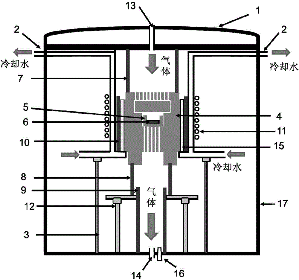
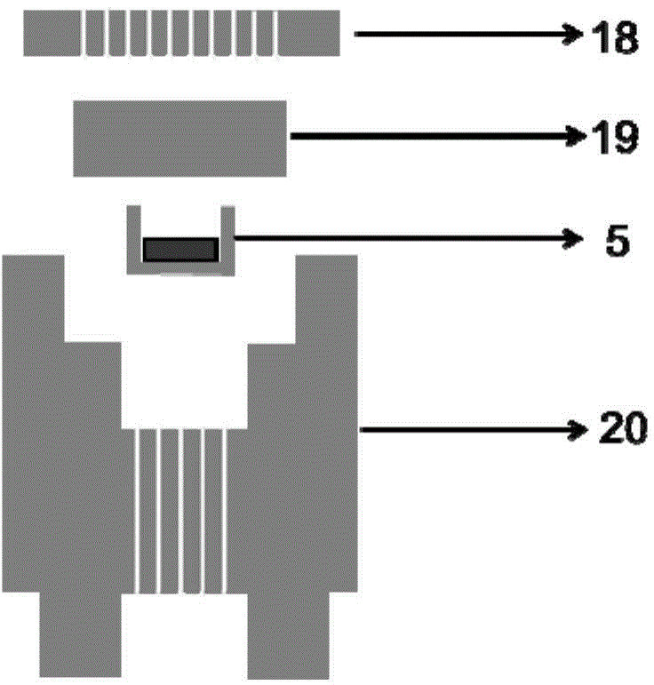
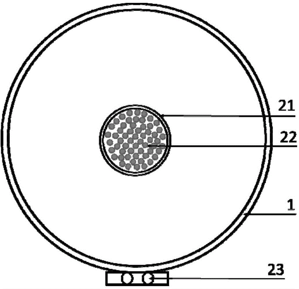
[0058] Example 1: A device for preparing graphene single crystals on a SiC substrate using high-temperature CVD technology. The gas inlet and outlet of the device adopt the upper and lower convection mode, and the structure is as follows figure 1 As shown, above the housing 17 is a top cover 1 with an air inlet 13 in the middle, and the gas nozzle 21 with a gas distribution pipe 22 arranged in the top cover 1 is connected, so that the incoming high-purity gas is evenly distributed into the reaction chamber; The cavity is located in the middle of the shell and consists of sealed quartz tubes 7 and 8, a graphite heating element 4 plugged in between the two sealed quartz tubes, and a graphite crucible 5 placed inside the graphite heating element. The graphite crucible 5 is used to place SiC Wafer substrate 6; the reaction chamber is supported by a stainless steel support frame 12 fixed on the bottom of the housing; the graphite heating element 4 has a thermal insulation layer 15;...
Embodiment 2
[0060] Embodiment 2: utilize the apparatus of embodiment 1 to carry out graphene crystal growth on 6H-SiC substrate
[0061] 1. Put the cut and cleaned 6H-SiC substrate on the graphite crucible 5, pass the inert gas Ar gas into the reaction chamber, raise the temperature from room temperature to 800°C within 90s, and keep it warm for 90s, and the Ar gas flow rate is 500sccm. Then the temperature was raised from 800°C to 1150°C within 30s and kept at 1150°C for 60s.
[0062] 2. Then pass high-purity H into the reaction chamber 2 , at the same time at a speed of 300-600°C / min, the temperature is rapidly raised to 1500°C to etch the SiC substrate, H 2 The flow rate is 800 sccm and the duration is 15 min.
[0063] 3. Cool down the SiC that has been etched in step 2 to 900°C at a cooling rate of 300-800°C / min, keep it at this temperature for 5 minutes, and cut off the H 2 Air flow, vacuumize the cavity.
[0064] 4. Heat up the SiC wafer obtained in step 3 to 1550°C at a rate of...
Embodiment 3
[0068] As described in Example 2, the difference is:
[0069] In step 1, the 6H-SiC substrate is placed on the graphite crucible 5, the reaction chamber is filled with inert gas Ar gas, the temperature is raised from room temperature to 800° C. within 90 s, and the temperature is kept for 90 s, and the flow rate of Ar gas is 500 sccm. Then the temperature was raised from 800°C to 1150°C within 30s and held for 90s.
[0070] In step 2, high-purity H is passed into the reaction chamber 2 , at a rate of 400°C / min, the temperature is rapidly raised from 1150°C to 1550°C for etching, H 2 The flow rate is 800 sccm and the duration is 10 min.
[0071] Step 3 is the same as in Example 1.
[0072] Step 4: Rapidly raise the temperature to 1525°C at a rate of 500°C / min, and keep the temperature at this temperature for 5 minutes to partially break the Si-C bond on the surface of SiC, and obtain the carbon source nucleation point for growing graphene. Introduce a large amount of Ar gas...
PUM
 Abstract
Description
Claims
Application Information


