Flip LED chip preparation method

A technology of LED chips and LED epitaxial wafers, which is applied in the direction of electrical components, circuits, semiconductor devices, etc., can solve the problems of uncontrollable over-thick metal, leakage, and dirty corrosion, achieve good current expansion effect, improve brightness, and avoid Unicom Effect

Inactive Publication Date: 2015-06-10
西安利科光电科技有限公司
View PDF5 Cites 10 Cited by
  • Summary
  • Abstract
  • Description
  • Claims
  • Application Information

AI Technical Summary

Problems solved by technology

[0004] The use of DBR reflectors for ultraviolet LED chips can further improve the brightness of the chip. In the prior art, the back of the LED chip is coated with a DBR reflector, and the flip chip uses a thick metal reflective layer combined with a silicon dioxide passivation layer to form a reflector. , the use of thick Ag technology as a reflector not only absorbs light (especially deep ultraviolet light), but also when corroding thick Ag during processing, the liquid corrosion has the same characteristics. Too thick metal is not easy to control, and it is easy to cause poor corrosion. clean and leakage

Method used


Image

  • Flip LED chip preparation method
  • Flip LED chip preparation method

Examples


preparation example Construction

[0034] 1) Preparation of P-type ohmic contact layer: Ni / Ag thin film evaporation is carried out using a vacuum coating machine, and the evaporation rate of Ni is The evaporation thickness is The Ag evaporation rate is The evaporation thickness is Forming a P-type ohmic contact layer;

[0035] 2) Perform coating, exposure, development and film hardening on the wafer to form the pattern required for the flip-chip mirror. The distance between the area covered by the photoresist and the N-type gallium nitride area exposed after etching is 7-10 μm , followed by H 2 O:NH 4 F:H 2 o 2 =5:1:1 solution corrosion for 3min, HCl:HNO 3 =3:1 solution etch for 3min, then remove the photoresist;

[0036] 3) P-type ohmic contact layer annealing: annealing in a rapid annealing furnace, annealing at 500 ° C for 1 min;

[0037] 4) Preparation of high ultraviolet reflectance reflector: Evaporate DBR reflective layer, made of SiO 2 with TiO 2 , first deposit a layer of SiO 2 Thickness ...

Embodiment 1

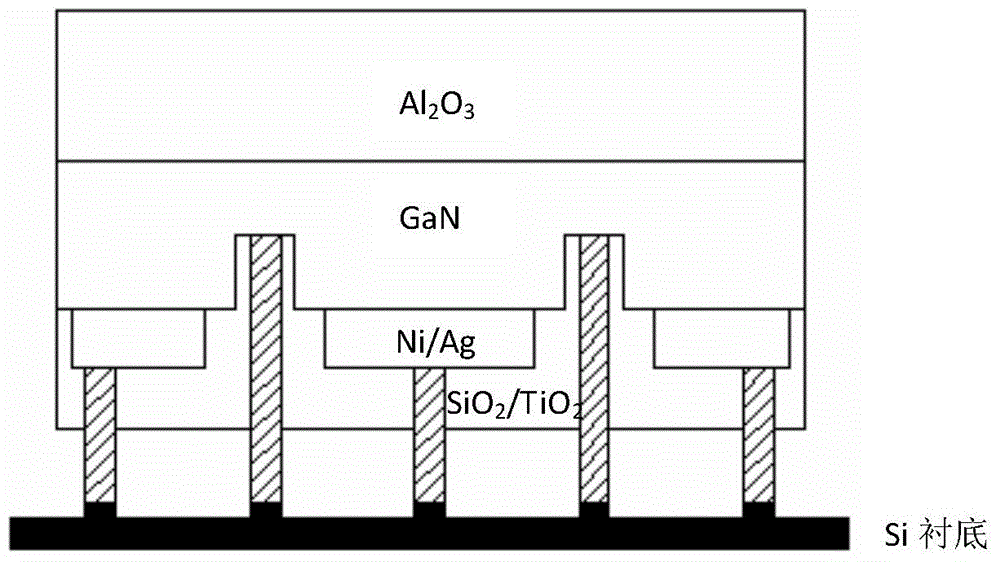
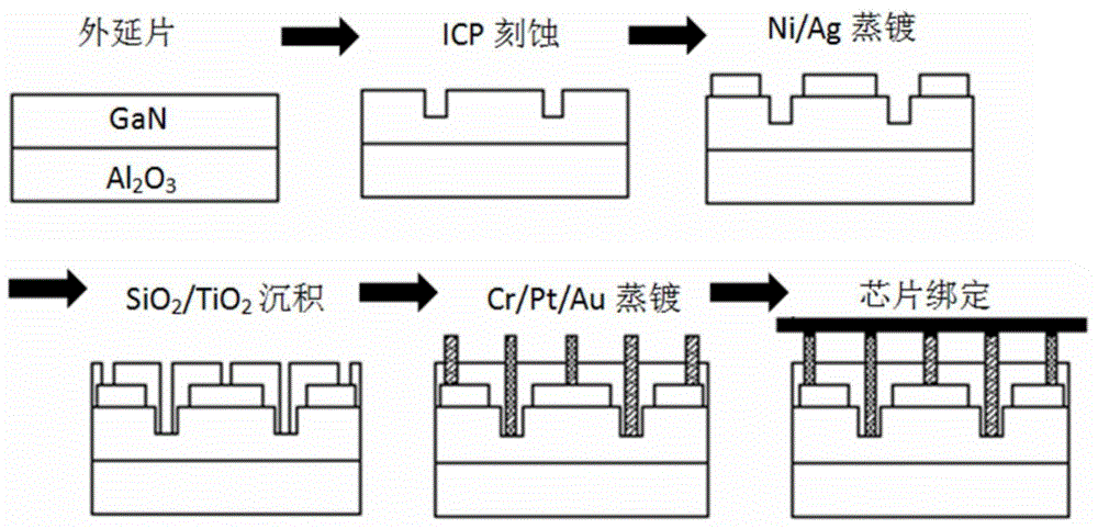
[0043] The flip-chip LED chip structure of the present invention is as figure 1 . Its preparation process is as follows figure 2 As shown, using ICP etching, Ni / Ag evaporation, SiO 2 / TiO 2 deposition, Cr / Pt / Au evaporation and die bonding processes. The present invention is mainly aimed at flip-chip ultraviolet LED chips, and the specific manufacturing process is as follows:

[0044] 1. Use aqua regia (HNO 3 : HCl=1:3) for surface treatment for 10 minutes, rinse with deionized water and dry;

[0045] 2. Put it into the ICP equipment for low-damage ultraviolet gallium nitride etching technology, and etch the P-type gallium nitride layer and the underlying multi-quantum well light-emitting layer in some areas of the epitaxial wafer, exposing the N-type gallium nitride layer, and etching etch using Cl 2 The flow rate is 50sccm, the Antenna RF power is 150W, the Bias RF power is 40W, and the etching depth is 1.3μm;

[0046] 3. The thin film evaporation machine performs Ni...

Embodiment 2

[0055] Embodiment 2 (this embodiment is suitable for preparing Blu-ray chip)

[0056] The thin film evaporation machine performs Ni / Ag thin film evaporation, and the Ni evaporation rate is Evaporation thickness The Ag evaporation rate is Evaporation thickness When evaporating, the vacuum degree is higher than 2.0×10⁻⁶Torr; nitrogen protection annealing, annealing temperature 400 ℃, annealing time 8min; deposit a layer of SiO2 thickness of Then TiO2 and SiO2 films are deposited alternately to form a multi-period structure, the number of periods is 8, and the deposition thickness of TiO2 films in 8 periods is the same as The thickness of SiO2 in 8 cycles is the same as The rest of the processes are the same as those in the first embodiment, and a flip-chip blue LED chip can be prepared. (The main difference between the blue light chip and the purple light chip is: the thickness of Ag in the Ni / Ag film is thicker than that of the purple light chip, and the reflectivit...


PUM

PropertyMeasurementUnit
wavelengthaaaaaaaaaa
reflectanceaaaaaaaaaa

Abstract

The invention discloses a novel flip LED chip preparation method. The novel flip LED chip preparation method is used for preparing a high-reflectivity reflector and the related structure. Through combining an ultra-thin Ni/Ag film with a DBR reflector, the light absorption of the metal can be reduced, the chip brightness is effectively improved, and meanwhile, the DBR reflector replaces a traditional silicon oxide passivation layer to protect the chip. The evaporation rate of Ni in the Ni/Ag film is expressed in a FORMULA (as shown in the description), the evaporation thickness is expressed in a FORMULA (as shown in the description), the evaporation rate of Ag is FORMULA (as shown in the description), and the evaporation thickness is expressed in a FORMULA (as shown in the description); a DBR reflecting layer comprises single-layer SiO2 and a multi-period structure formed by alternately depositing TiO2 and SiO2 films based on the single-layer SiO2, and the period number is larger than 4.

Description

Technical field: [0001] The invention belongs to the technical field of LED chip preparation, and mainly relates to a new preparation method for improving the brightness of flip-chip LED chips. Background technique: [0002] With the development of LED applications, UV LEDs are widely used because of their wider spectral range (light emitting wavelengths can cover the 210-400nm band), more energy-saving, and no toxic mercury. In many aspects of life, such as UV disinfection, UV hardening, optical sensors, UV authentication, body fluid detection and analysis and other fields. The current main challenge of UV LED technology is the chip with low efficiency and wavelength below 365nm, and the output power of UV LED is only 5%-8% of the input power. When the wavelength is above 385nm, the efficiency of violet LED is improved, but only 15% of the input power. [0003] Flip-chip LED chips can effectively improve the brightness of LED chips. Traditional flip-chips are mainly blue...

Claims


Application Information

Patent Timeline
Patent Type & Authority Applications(China)
IPC IPC(8): H01L33/44H01L33/46H01L33/14H01L33/00
Inventor 宁磊
Owner 西安利科光电科技有限公司
Why Eureka
Try Eureka