CMOS (complementary metal-oxide semiconductor) infrared detector reading-out circuit capable of realizing element-by-element dark current suppression

An infrared detector and dark current suppression technology, applied in the direction of electric radiation detectors, etc., can solve the problem of small output swing of the circuit, achieve the effects of improving nonlinearity, ensuring repeatability, and reducing inhomogeneity

Active Publication Date: 2015-07-01
SHANGHAI INST OF TECHNICAL PHYSICS - CHINESE ACAD OF SCI
View PDF4 Cites 7 Cited by
  • Summary
  • Abstract
  • Description
  • Claims
  • Application Information

AI Technical Summary

Problems solved by technology

[0004] The purpose of the present invention is to provide a CMOS infrared detector readout circuit with element-by-element dark current suppression, which solves the problem that the outpu...

Method used


Image

  • CMOS (complementary metal-oxide semiconductor) infrared detector reading-out circuit capable of realizing element-by-element dark current suppression
  • CMOS (complementary metal-oxide semiconductor) infrared detector reading-out circuit capable of realizing element-by-element dark current suppression
  • CMOS (complementary metal-oxide semiconductor) infrared detector reading-out circuit capable of realizing element-by-element dark current suppression

Examples


Embodiment approach 1

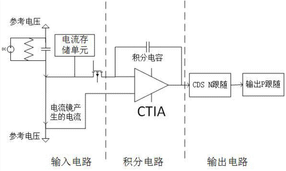
[0022] This invention adopts the combination of current storage unit and current mirror at the input end to design the medium and long-wave infrared detector line column readout circuit, and its unit structure diagram is as follows figure 1 As shown, one end of the medium and long-wave infrared detector is connected to the reference voltage, and the other end is connected to the input end of the CTIA amplifier; the reference voltage is the initial voltage of CTIA integration, which is generally set to 1.5V, and the minimum can not be lower than the threshold voltage of the NMOS tube, otherwise Distortion occurs at the low end of the signal. C i It is an integral capacitor, which can be selected according to the responsivity of the medium and long-wave infrared detectors; in order to make the detector signals of the line array read out sequentially, it is necessary to add CDS N follower to the output end of CTIA, and then connect P follower. The readout of the circuit is divid...

Embodiment approach 2

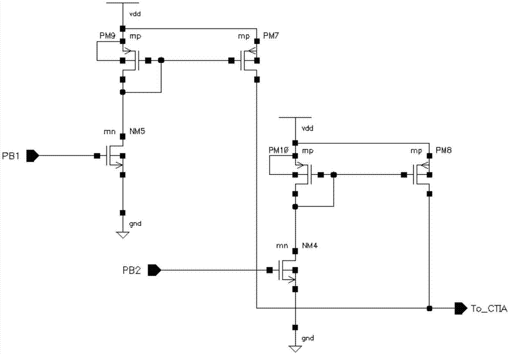
[0024] The circuit structure of the circuit in the input current mirror mode is as follows figure 2 As shown, since the width-to-length ratio of PM9 is twice that of PM10, and the width-to-length ratio of NM4 is 8 times that of NM5, PM8 and PM10 constitute the input-stage current mirror for coarse-tuning control, and PM7 and PM9 constitute the input-stage current for fine-tuning control Mirror, PB1, PB2 are fine-tuning, coarse-tuning external ports respectively. When drawing the layout, the current mirror is arranged at the left and right ends of the column circuit, and the ground wire adopts a metal wire with a width greater than 100 microns. The non-linearity of the line array 160 circuit designed by this method is less than 1%.

[0025] The tube reference size of the current mirror part is shown in the table below (unit is micron).

[0026] the pipe

Embodiment approach 3

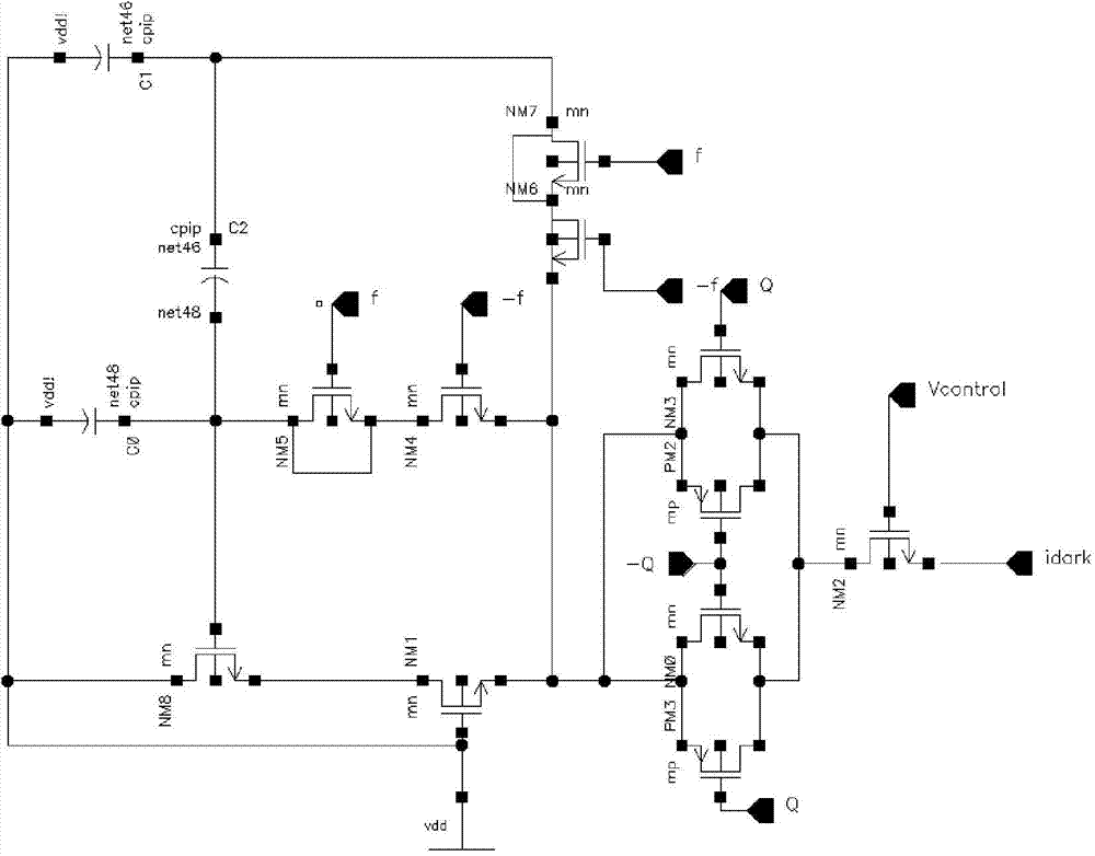
[0028] The structure of the current storage unit at the input end of the circuit is as follows: image 3 As shown, NM8 is used as a storage tube, the current flowing through it is equal to the external dark current, and the gate voltage of NM8 tube is stored by the capacitor feedback loop, so as to achieve the purpose of storing dark current. The capacitive feedback loop is composed of capacitors C0, C1, and C2, whose capacitance values ​​are 2pF, 20fF, and 2pF respectively, which can effectively reduce the feedthrough voltage, and the rejection ratio is C0 / C1=100. NM4 / NM5 and NM6 / NM7 form two pairs of virtual switches, which are controlled by the pulse signal f / -f to reduce the influence of channel charge injection on the capacitive feedback loop. PM2 / NM3 and PM3 / NM0 form a transmission gate switch, and the reference size of each tube is shown in the table below (unit is micron).

[0029] the pipe


PUM

PropertyMeasurementUnit
Widthaaaaaaaaaa

Abstract

The invention discloses a CMOS (complementary metal-oxide semiconductor) infrared detector reading-out circuit capable of realizing element-by-elementdark current suppression. The CMOS infrared detector reading-out circuit comprises input circuit, an integration circuit and an output circuit, the input circuit is of a structure combining current storage units with current mirrors, the current storage units are distributed in each pixel of a linear array circuit, each current storage unit is composed of a transmission gate, a virtual switch pair and a capacitance coupling loop, and customized modulation of dark current can be realized; the current mirrors are arranged at the left end and right end of the linear array circuit, and integral suppression of dark current can be realized. The CMOS infrared detector reading-out circuit has the advantages that the current storage units at an input end are designed, so that detector signal heterogeneity can be lowered effectively; the current mirrors at the input end are provided with a rough tuning port and a fine tuning port, so that scope of application, to medium-long-wave infrared detector working current, of the CMOS infrared detector reading-out circuit is expanded, and working state of a system can be adjusted accurately; the CMOS infrared detector reading-out circuit is low in power consumption, and is manufactured by adopting a submicron CMOS process, thereby being high in repeatability.

Description

technical field [0001] The invention relates to the field of readout circuits of infrared detectors, in particular to a design of CMOS readout circuits for line array medium and long wave infrared detectors. Background technique [0002] Mid- and long-wave infrared detectors have extremely important uses in the fields of low-temperature target detection, over-the-horizon detection, and anti-jamming target recognition, so they have always been an important direction for the development of infrared detector technology. At present, medium-wave detectors (with a wavelength of 3.5-4 μm) are still dominated by HgCdTe detectors, which generally work in a high background and will generate a large background current. At the same time, the dark current of the HgCdTe medium-long-wave infrared device itself is relatively large, and there is relatively large non-uniformity. When the signal is read out, the signal of each element is prone to unevenness, and some signals cannot be read out...

Claims


Application Information

Patent Timeline
IPC IPC(8): G01J5/10
Inventor 宋伟清袁红辉周廉白涛
Owner SHANGHAI INST OF TECHNICAL PHYSICS - CHINESE ACAD OF SCI
Why Eureka
Try Eureka