Method for depositing high-K gate dielectric on atomic layer on surface of graphene

A graphene surface and atomic layer deposition technology, which is applied in the direction of electrical components, semiconductor/solid-state device manufacturing, circuits, etc., can solve the problem of inability to ensure good contact between the metal and the bottom graphene, and the inability to deposit high-k gate dielectrics and graphene lattices Damage and other problems, to achieve the effect of tight combination, good uniformity and continuity, and small lattice damage

Inactive Publication Date: 2015-08-19
XIAN JIAOTONG LIVERPOOL UNIV
View PDF3 Cites 5 Cited by
  • Summary
  • Abstract
  • Description
  • Claims
  • Application Information

AI Technical Summary

Problems solved by technology

[0004]However, the deposition of high-k materials on graphene materials still faces two problems: 1) The large π bonds on the surface of graphene cause it to have no chemical The dangling bonds necessary for the adsorption of precursor sources are chemically inactive and cannot directly deposit high-k gate dielectrics on graphene; 2) In order to deposit high-k gate dielectrics on graphene, graphene is generally pretreated before deposition
Generally, electron beam evaporation is used to pretreat graphene by depositing a metal seed layer on graphene, but this method will cause great damage to the graphene lattice.
Some methods are to re-grow a layer of island-shaped graphene on the flat and defect-free graphene surface. The disadvantage is that the process is cumbersome, and during the growth process, good contact between the metal used for growth and the bottom graphene cannot be guaranteed.
However, the method of applying an electric field in the ALD reaction chamber will become difficult due to the limitations of the ALD reaction equipment itself, and it is difficult to realize it in a real sense.
In addition, the use of scanning electron microscopy (SEM) to grow amorphous carbon films requires additional equipment and high cost

Method used


Image

  • Method for depositing high-K gate dielectric on atomic layer on surface of graphene
  • Method for depositing high-K gate dielectric on atomic layer on surface of graphene
  • Method for depositing high-K gate dielectric on atomic layer on surface of graphene

Examples


Embodiment Construction

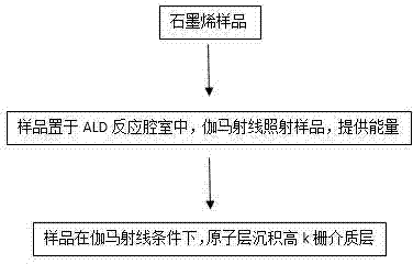
[0028] In order to make the object, technical solution and advantages of the present invention clearer, the present invention will be further described in detail below in combination with specific embodiments and with reference to the accompanying drawings. In this example, only Al 2 O 3 gate dielectric layer, but the dielectric layer is not doped. It should be understood that these descriptions are exemplary only, and are not intended to limit the scope of the present invention. Also, in the following description, descriptions of well-known structures and techniques are omitted to avoid unnecessarily obscuring the concept of the present invention.

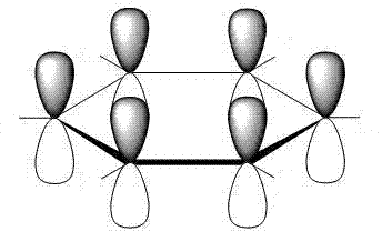
[0029] figure 1 It is a schematic diagram of the S orbitals between the six carbon atoms of graphene and the six P orbitals perpendicular to the two-dimensional plane.

[0030] The rays used in this example are gamma rays but are not limited to gamma rays, other rays can also be used, and the method of the presen...


PUM


Abstract

The invention discloses a method for depositing high-K gate dielectric on an atomic layer on the surface of graphene, comprising the following steps: preparing a graphene material with a clean and smooth surface and few defects as a substrate sample for depositing high-k gate dielectric; putting the substrate sample in an ALD reaction chamber, and remotely controlling rays to make electron absorption energy of a P orbit of graphene jump, change outer electron orientation, damage a delocalized large-Pai bond and form a dangling bond; feeding water vapor to complete chemical adsorption on the surface of graphene until the surface of the substrate is saturated; and feeding a first precursor source to complete high-k gate dielectric deposition on the surface of graphene. According to invention, gamma rays are used to excite electrons and damage a delocalized large-Pai bond so as to improve the surface activity of graphene. The method for depositing high-K gate dielectric on an atomic layer on the surface of graphene is simple to implement and reliable. By adopting the method, a continuous, uniform and closely-combined high-k gate dielectric layer can be formed directly on the surface of graphene.

Description

technical field [0001] The invention belongs to the field of carbon-based integrated circuits, and in particular relates to a method for using radiation to excite electrons to deposit a high-k grid dielectric on the surface of graphene. Background technique [0002] With the development of the field of integrated circuits, the size of devices in the field of microelectronics is decreasing day by day, and the development of silicon-based integrated circuits originally used has reached a bottleneck. It is almost impossible to reduce the processing line width without degrading the performance of the product. More excellent new materials urgently need to be developed and applied. [0003] In order to reduce the device size while obtaining better integrated circuit devices, graphene, as a new type of material, has high expectations. Its ultra-high carrier mobility, excellent mechanical properties, thermal stability and good semiconductor properties make Graphene has become the f...

Claims


Application Information

Patent Timeline
IPC IPC(8): H01L21/285
Inventor 吴京锦慕轶非赵策洲汤楚帆
Owner XIAN JIAOTONG LIVERPOOL UNIV
Why Eureka
Try Eureka