Medium-frequency magnetron reactive sputtering method for aluminum nitride film

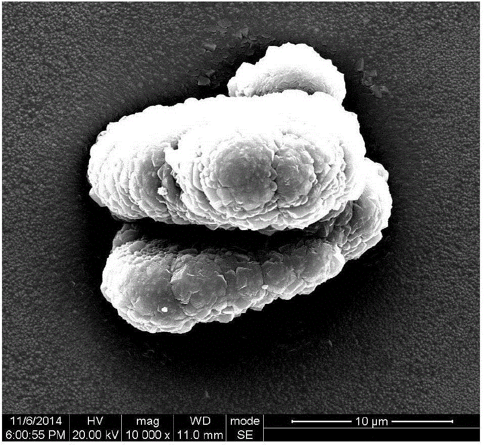
A technology of aluminum nitride and thin film, which is applied in the field of piezoelectric thin film manufacturing, can solve problems such as the influence of aluminum nitride thin film quality, grain growth on the film surface, and device performance failure, and achieve normal grain growth on the surface, smooth surface, The effect of uniform grain size

Inactive Publication Date: 2015-08-26
UNIV OF ELECTRONICS SCI & TECH OF CHINA
View PDF10 Cites 15 Cited by
  • Summary
  • Abstract
  • Description
  • Claims
  • Application Information

AI Technical Summary

Problems solved by technology

[0004] However, in the intermediate frequency reactive sputtering technology, the sputtering process parameters have a great influence on the growth quality of the aluminum nitride film. The surface temperature of the film caused by the bombardment of the plasma and the sputtered aluminum particles on the film surface is too high, and the relatively high Large sputtering power will make the crystal grains on the surface of the film grow abnormally, and some micron-submicron aluminum nitride large particles will appear on the film surface
This will have a great impact on the quality of the aluminum nitride film. The uneven grain size will affect the piezoelectric performance and the acoustic wave propagation rate of the aluminum nitride film, and the micron-submicron large particles on the surface will affect the next step. The manufacture of surface acoustic wave devices has brought catastrophic consequences, causing the interdigital electrode (IDT) of the surface acoustic wave device to break or short circuit, resulting in device performance failure

Method used


Image

  • Medium-frequency magnetron reactive sputtering method for aluminum nitride film
  • Medium-frequency magnetron reactive sputtering method for aluminum nitride film
  • Medium-frequency magnetron reactive sputtering method for aluminum nitride film

Examples


Embodiment Construction

[0023] The present invention will be further described below in conjunction with specific steps and accompanying drawing with a special example:

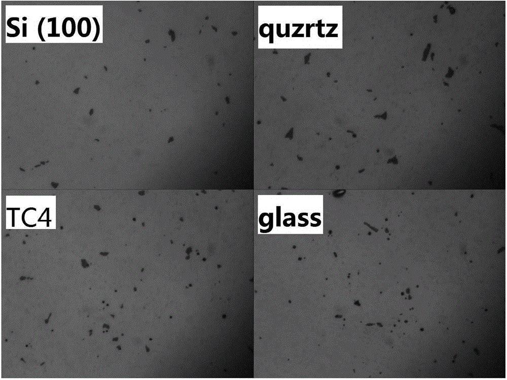
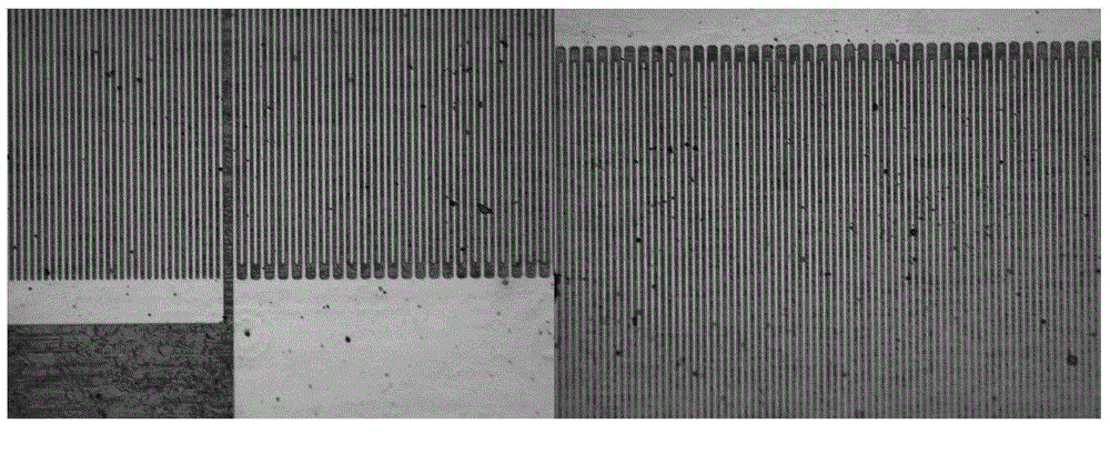
[0024] 1. Substrate cleaning: In the experiment, we used four different substrates, finely polished silicon (Si(100)) substrate, finely polished titanium alloy (TC4) substrate, ordinary glass substrate (glass), fine Polished quartz (quartz) substrate. Use acetone, alcohol, and deionized water to ultrasonically clean the surface of the substrate in sequence. After each cleaning for 15 minutes, dry the cleaned substrate with a nitrogen gun, put it into a drying box filled with pure nitrogen, and heat it to 100°C. °C for 1 hour.

[0025] 2. Vacuum pretreatment: place the four substrates processed in step 1 on the sample stage of the intermediate frequency magnetron reactive sputtering system, and close the cavity. Start the magnetron sputtering instrument normally, and evacuate the cavity to 5×10 -4 Below Pa.

[0026] 3. Pre-sputte...


PUM

PropertyMeasurementUnit
densityaaaaaaaaaa
electrical resistivityaaaaaaaaaa
electromechanical coupling coefficientaaaaaaaaaa

Abstract

The invention relates to the field of manufacture of piezoelectric films, in particular to a medium-frequency magnetron reactive sputtering method for an aluminum nitride film. According to a film deposition process, firstly, high-purity argon and high-purity nitrogen are fed simultaneously into a vacuum cavity, the content of the nitrogen is kept to range from 20% to 30%, and sputter deposition of the aluminum nitride film is started after glow is stabilized; then the proportion of the argon to the nitrogen in the sputtering cavity is adjusted at the constant speed of 0.5 sccm/min-4 sccm/min in 10-20 min, and the content of the nitrogen is increased to 50% from the previous 20%-30%; finally, the sputtering power is not adjusted, sputter deposition of aluminum nitride is performed in the atmosphere for 10 min, an instrument is shut down, and film growth is ended. With the adoption of the method, the high-quality aluminum nitride piezoelectric film which meets the requirements for satisfaction of C-axis preferred orientation growth, normal surface grain growth, the uniform grain size, the smooth surface and suitability for producing a surface acoustic wave device can be prepared.

Description

Technical field: [0001] The invention relates to the field of piezoelectric thin film manufacturing, in particular to an intermediate frequency magnetron reactive sputtering method for aluminum nitride thin films. Background technique: [0002] Aluminum nitride (AlN) is the only stable compound formed by aluminum (Al) and nitrogen (N), and it is a typical III-V compound semiconductor. Its unit cell belongs to the hexagonal wurtzite structure, which is a deformed tetrahedron with an aluminum atom as the center and four nitrogen atoms around the outside. Aluminum nitride has a series of excellent physical and chemical properties, such as: large band gap (6.2eV); high thermal conductivity (320W / m K); low density (3.26g / cm 3 ); large resistivity (10 13 Ω cm); high thermal stability (surface oxidation occurs above 700°C); high surface acoustic wave propagation velocity (12000m / s along the C axis, 6000m / s perpendicular to the C axis); large electromechanical coupling Coefficien...

Claims


Application Information

Patent Timeline
Patent Type & Authority Applications(China)
IPC IPC(8): C23C14/35C23C14/06
Inventor 彭斌姜建英张万里张文旭王睿邓言文
Owner UNIV OF ELECTRONICS SCI & TECH OF CHINA
Why Eureka
Try Eureka