Photoelectric synchronous sensing method of solid-state nanochannels based on dark-field imaging

A nano-channel and dark-field imaging technology, applied in the field of electrochemical analysis technology and nano-spectroscopy, can solve the problems of influence of motion behavior, complicated labeling process, influence of single-molecule analysis results, etc., and achieve the effect of expanding the application field and accelerating the detection rate.

Inactive Publication Date: 2017-11-03
EAST CHINA UNIV OF SCI & TECH
View PDF6 Cites 0 Cited by
  • Summary
  • Abstract
  • Description
  • Claims
  • Application Information

AI Technical Summary

Problems solved by technology

At present, the technology for photoelectric synchronous reading of nanochannels requires the introduction of dye groups, which will not only affect the movement behavior of the analyte at the level of a single molecule and a single particle, but also the labeling process is complicated. The failure of bleaching and labeling will affect the analysis results of single molecules

Method used


Image

  • Photoelectric synchronous sensing method of solid-state nanochannels based on dark-field imaging
  • Photoelectric synchronous sensing method of solid-state nanochannels based on dark-field imaging
  • Photoelectric synchronous sensing method of solid-state nanochannels based on dark-field imaging

Examples


Embodiment 1

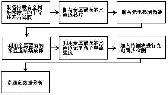
[0050] The photoelectric synchronous sensing method of the solid-state nano channel based on dark field imaging comprises the following steps (see figure 1 ):

[0051](1) Preparation of semiconductor substrate film coated with metal nano-coating

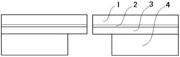
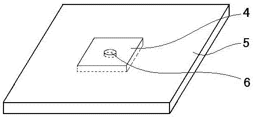
[0052] ① Deposit a layer of 100nm-thick silicon nitride film 3 on the single crystal silicon wafer by chemical vapor deposition technology of micromachining technology, and then use photolithography to etch squares with a side length of 200 microns and a spacing of 5 mm on one side of the single crystal silicon wafer. The window 4 exposes the silicon nitride film 3; the silicon circle is cut to obtain a substrate 5 containing a single square window 4.

[0053] The micro-processing technology includes chemical vapor deposition, photolithography, chemical etching, electron beam exposure, reactive ion beam etching, magnetron sputtering, electron beam evaporation, atomic layer deposition, molecular beam epitaxy, laser sputtering deposit...

Embodiment 2

[0097] A photoelectric synchronous sensing method of a solid-state nanochannel based on dark-field imaging, comprising the following specific steps:

[0098] (1) Prepare a semiconductor substrate film coated with a metal nano-coating (same as Example 1).

[0099] (2) Preparation of a metal-coated nanochannel chip (same as in Example 1).

[0100] (3) Prepare a photoelectric detection microcell (same as Example 1).

[0101] (4) Dark-field imaging using metal-coated nanochannels

[0102] Perform dark-field imaging on the metal-coated nanochannel chip 9 and continuously monitor the changes in its spectrum within a certain period of time. The specific content is:

[0103] ① Place the photoelectric detection microcell on the microscope stage, perform dark-field illumination through the dark-field lens, use a 100 W halogen lamp as the white light source, and use the microscope imaging device to image on the first color CCD camera.

[0104] ② Convert the optical path so that all th...


PUM

PropertyMeasurementUnit
thicknessaaaaaaaaaa
thicknessaaaaaaaaaa
thicknessaaaaaaaaaa

Abstract

The photoelectric synchronous sensing method of the solid-state nano-channel based on dark-field imaging of the present invention comprises the following steps: (1) preparing a semiconductor substrate film coated with a metal nano-coating; (2) preparing a metal-coated nano-channel chip; (3) preparing a photoelectric detection micro (4) using metal-coated nano-channel dark-field imaging; (5) using metal-coated nano-channel to record ion current intensity; (6) adding the object to be tested for photoelectric synchronous detection; (7) multi-channel data analysis. The invention adopts the method of photoelectric synchronous sensing, without introducing dye groups, and without labeling, it can monitor the process of a single nanometer object passing through the nanochannel in real time, and realize the volume, charging situation, optical properties, chemical structure, etc. of the object to be measured. The collection of dynamic information can observe the changes of various properties of a single object under test during its movement from multiple dimensions; it realizes the simultaneous acquisition of large-scale multi-channel signals, accelerates the detection rate of nano-channel technology, and expands its application field.

Description

technical field [0001] The invention relates to the fields of electrochemical analysis technology and nanometer spectrum technology, in particular to a method for realizing synchronous sensing of nanochannel photoelectric signals by using plasmon resonance scattering combined with ion current detection technology. Background technique [0002] Nanopore Electrochemical Detection Technology (Nanopore Technique) is a single-molecule analysis technology that uses biomolecular self-assembly or semiconductor microfabrication to obtain nanopores with a pore size ranging from 1 nanometer to hundreds of nanometers, and then uses an electric field to drive a single molecule , nanoparticles, polymers and other analytes pass through nanometer-sized channels, which will cause weak signal changes in nanochannels, and study the composition and motion of analytes at the single-molecule and single-particle level to achieve real-time, real-time analysis of single molecules. High-throughput, l...

Claims


Application Information

Patent Timeline
Patent Type & Authority Patents(China)
IPC IPC(8): G01N21/69
Inventor 龙亿涛师鑫高瑞应佚伦静超李好问
Owner EAST CHINA UNIV OF SCI & TECH
Why Eureka
Try Eureka