Method for preparing field emission cathode of nano carbon sheet-silicon nanowire composite structure

A field emission cathode and silicon nanowire technology, which is applied in the preparation and application of nanomaterials, can solve the problems of poor field electron emission ability and difficult to work stably

Inactive Publication Date: 2015-09-02
TIANJIN NORMAL UNIVERSITY
View PDF2 Cites 7 Cited by
  • Summary
  • Abstract
  • Description
  • Claims
  • Application Information

AI Technical Summary

Problems solved by technology

[0005] The purpose of the present invention is to overcome the existing field emission cathode based on silicon nanowires with high open field, small field emission current density, and field emission current density greater than 1 mA / cm2 is difficult to work stably. A simple plasma-enhanced chemical vapor deposition process is used to grow densely distributed nanoscale carbon sheets on silicon nanowires, so that the field on silicon nanowires The number of emission points is greatly increased, thereby providing a silicon nanowire substrate with low turn-on field, greatly increased field emission current density, and stable field electron emission when the field emission current density is greater than 1 mA / cm2 Composite Field Emission Cathode Materials

Method used


Image

  • Method for preparing field emission cathode of nano carbon sheet-silicon nanowire composite structure
  • Method for preparing field emission cathode of nano carbon sheet-silicon nanowire composite structure
  • Method for preparing field emission cathode of nano carbon sheet-silicon nanowire composite structure

Examples


Embodiment 1

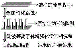
[0035] (1) Preparation of clean silicon wafer substrate:

[0036] First, cut the silicon wafer into small pieces of 2cm×2cm, clean them with ultrasonic (50W) in deionized water, acetone and absolute ethanol for 10 minutes, and then put the silicon wafer into hydrofluoric acid with a volume ratio of 4% for 5 minutes. Minutes for clean, contamination-free substrates free of silica overlays.

[0037] (2) Fabrication of silicon nanowire arrays by metal-catalyzed corrosion method:

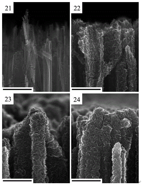
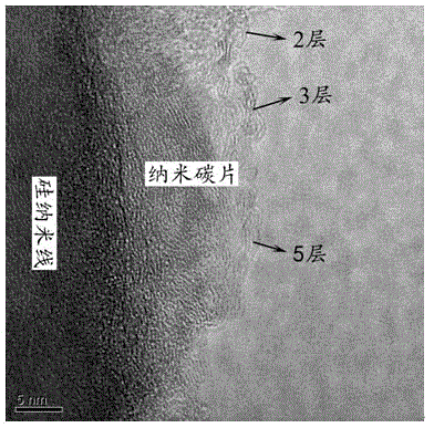
[0038] The metal-catalyzed corrosion method is a conventional method for preparing silicon nanowire arrays: firstly, the cleaned silicon wafer is placed in a AgNO 3 :HF:H 2 O = 2:10:38 solution soaked for 1 minute, used to deposit the silver catalyst; then immediately put the silicon wafer deposited with the silver catalyst particles into the volume ratio of H 2 o 2 :HF:H 2 The silicon nanowires were grown by soaking and etching in the solution of O=1:10:39 for 45 minutes, and the silicon nanowire ...

Embodiment 2

[0046] (1) Preparation of clean silicon wafer substrate:

[0047] First, cut the silicon wafer into small pieces of 2cm×2cm, clean them with ultrasonic (50W) in deionized water, acetone and absolute ethanol for 10 minutes, and then put the silicon wafer into hydrofluoric acid with a volume ratio of 4% for 5 minutes. Minutes for clean, contamination-free substrates free of silica overlays.

[0048] (2) Fabrication of silicon nanowire arrays by metal-catalyzed corrosion method:

[0049] The metal-catalyzed corrosion method is a conventional method for preparing silicon nanowire arrays: firstly, the cleaned silicon wafer is placed in a AgNO 3 :HF:H 2 O = 2:10:38 solution soaked for 1 minute, used to deposit the silver catalyst; then immediately put the silicon wafer deposited with the silver catalyst particles into the volume ratio of H 2 o 2 :HF:H 2 The silicon nanowires were grown by soaking and etching in the solution of O=1:10:39 for 45 minutes, and the silicon nanowire ...

Embodiment 3

[0057] (1) Preparation of clean silicon wafer substrate:

[0058] First, cut the silicon wafer into small pieces of 2cm×2cm, clean them with ultrasonic (50W) in deionized water, acetone and absolute ethanol for 10 minutes, and then put the silicon wafer into hydrofluoric acid with a volume ratio of 4% for 5 minutes. Minutes for clean, contamination-free substrates free of silica overlays.

[0059] (2) Fabrication of silicon nanowire arrays by metal-catalyzed corrosion method:

[0060] The metal-catalyzed corrosion method is a conventional method for preparing silicon nanowire arrays: firstly, the cleaned silicon wafer is placed in a AgNO 3 :HF:H 2 O = 2:10:38 solution soaked for 1 minute, used to deposit the silver catalyst; then immediately put the silicon wafer deposited with the silver catalyst particles into the volume ratio of H 2 o 2 :HF:H 2 The silicon nanowires were grown by soaking and etching in the solution of O=1:10:39 for 45 minutes, and the silicon nanowire ...


PUM

PropertyMeasurementUnit
Diameteraaaaaaaaaa
Diameteraaaaaaaaaa
Maximum field emission current densityaaaaaaaaaa

Abstract

The invention discloses a method for preparing a field emission cathode of a nano carbon sheet-silicon nanowire composite structure, and belongs to the fields of preparation and application of nano materials. The method mainly includes the following preparation process of using a silicon nanowire array prepared on a clean silicon single crystal wafer by using a metal catalysis and corrosion method as a substrate; growing nano-scale carbon sheets on the substrate by using a microwave plasma enhanced chemical vapor deposition method; and finally using the obtained nano carbon sheet-silicon nanowire composite structure as a cathode assembly field electron emitter. As for the nano carbon sheet-silicon nanowire composite structure prepared by the method, the carbon sheets mostly have a diameter of 60-100nm, with generally 2-5 edge layers, and are distributed densely on the surface of silicon nanowires. As the field emission cathode material, the nano carbon sheet-silicon nanowire composite structure has a lower open field and a larger field emission current density than a single silicon nanowire array, and has a very high application value.

Description

[0001] The invention was funded by the National Natural Science Foundation of China -Youth Fund Project (Project No. 51302187).Receive the key project funding by Tianjin's application foundation and cutting -edge technology research plan (item number 14jczdjc32100). Technical field [0002] The present invention belongs to the field of preparation and application technology of nanomaterials, involving the use of plasma to enhance chemical gas deposition method to prepare a composite nanomaterial with a unique structure with a silicon nan navile.Essence Background technique [0003] As a semiconductor one -dimensional nanoma material, Silicon nanowine has a large long diameter ratio. It has certain application prospects in the field of electronic launch in the new generation of vacuum tube, X -ray tube, field launch tablet display.Compared with the traditional carbon nanotuba cathode material with the traditional field of launching performance with a silicon nano -line field, it ha...

Claims


Application Information

Patent Timeline
IPC IPC(8): H01J9/02
CPCB82Y30/00B82Y40/00C23C16/513H01J9/02H01J9/025
Inventor 邓建华程国安汪凡洁
Owner TIANJIN NORMAL UNIVERSITY
Why Eureka
Try Eureka