Organic electroluminescent device and preparation method thereof

An electroluminescent device and luminescent technology, which is applied in the fields of electric solid-state devices, semiconductor/solid-state device manufacturing, electrical components, etc., can solve the problem that the barrier performance of plastic substrates cannot reach OLED packaging, flexible packaging cannot be realized, and the surface of the cathode layer is damaged, etc. problems, to achieve the effect of easy large-area preparation and mass production, good bending stress and thermal stress, and reduced erosion

Inactive Publication Date: 2015-09-02
OCEANS KING LIGHTING SCI&TECH CO LTD +2
View PDF0 Cites 4 Cited by
  • Summary
  • Abstract
  • Description
  • Claims
  • Application Information

AI Technical Summary

Problems solved by technology

Flexible products are the development trend of organic electroluminescent devices, and the barrier properties of plastic substrates commonly used in flexible devices cannot meet the requirements of OLED packaging, so flexible organic electroluminescent devices generally have the problem of short life
At present, it has been reported that SiN x or SiO x Inorganic materials such as inorganic materials are arranged on the surface of the cathode layer by magnetron s

Method used


Image

  • Organic electroluminescent device and preparation method thereof
  • Organic electroluminescent device and preparation method thereof
  • Organic electroluminescent device and preparation method thereof

Examples


Embodiment 1

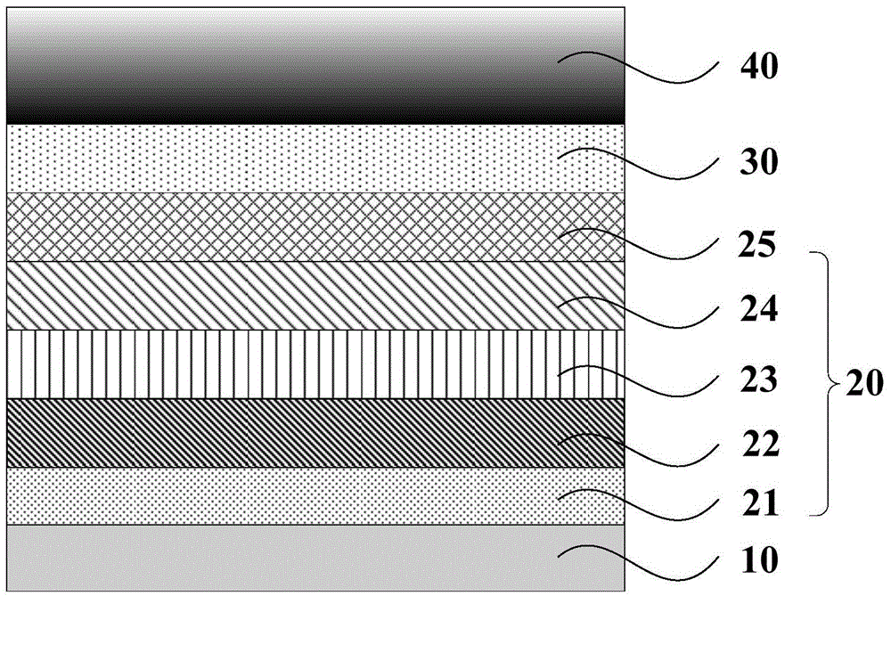
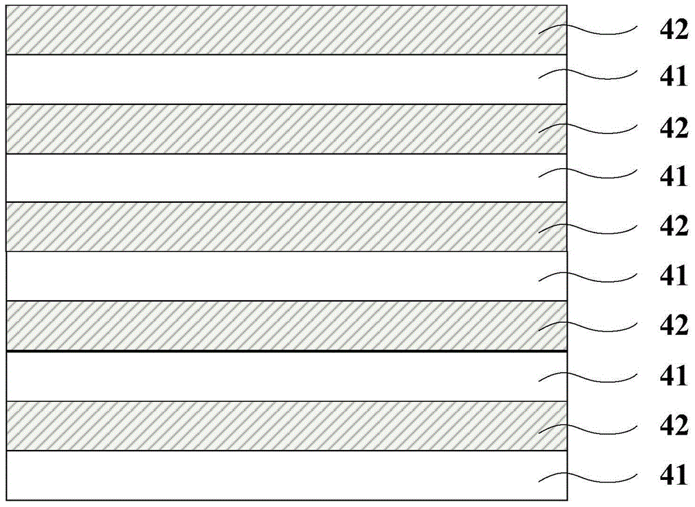
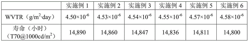
[0038] figure 1 It is a schematic structural diagram of an organic electroluminescent device provided in this embodiment. like figure 1 As shown, the organic electroluminescent device includes a conductive glass substrate 10 , an organic light-emitting functional layer 20 , a cathode layer 30 and an encapsulation layer 40 which are stacked sequentially from bottom to top. Wherein, the organic light-emitting functional layer 20 includes a hole injection layer 21 , a hole transport layer 22 , a light-emitting layer 23 , an electron transport layer 24 and an electron injection layer 25 stacked sequentially from bottom to top. figure 2 Yes figure 1 Schematic diagram of the structure of the encapsulation layer, such as figure 2 As shown, the encapsulation layer 40 includes an organic barrier layer 41 and an inorganic barrier layer 42 stacked in sequence, the organic barrier layer 41 and the inorganic barrier layer 42 form a structural unit, and the encapsulation layer 40 is co...

Embodiment 2

[0054] A method for preparing an organic electroluminescent device, comprising the following steps:

[0055] (1), (2) are the same as embodiment 1;

[0056] (3) Preparation of encapsulation layer:

[0057] (a) Preparation of organic barrier layer: The organic barrier layer was prepared on the surface of the cathode layer by plasma-enhanced chemical vapor deposition; CH 4 and N 2 As a reactive gas, control CH 4 The flow is 12sccm, N 2 The flow rate is 10sccm, the working pressure is 20Pa, and the RF power is 0.3W / cm 2 , the deposition thickness is 550nm;

[0058] (b) Preparation of the inorganic barrier layer: the inorganic barrier layer was prepared on the surface of the organic barrier layer by atomic layer deposition, the working pressure was controlled at 10Pa, and the deposition temperature was 40°C; the material of the inorganic barrier layer was Mg 3 N 2 ; Bis(ethylcyclopentadiene) beryllium (Mg(CpEt) 2 ) and NH 3 As a precursor, N 2 As carrier gas; controls Be...

Embodiment 3

[0063] A method for preparing an organic electroluminescent device, comprising the following steps:

[0064] (1), (2) are the same as embodiment 1;

[0065] (3) Preparation of encapsulation layer:

[0066] (a) Preparation of organic barrier layer: The organic barrier layer was prepared on the surface of the cathode layer by plasma-enhanced chemical vapor deposition; CH 4 and N 2 As a reactive gas, control CH 4 The flow rate is 8sccm, N 2 The flow rate is 10sccm, the working pressure is 60Pa, and the RF power is 0.4W / cm 2 , the deposition thickness is 450nm;

[0067] (b) Preparation of the inorganic barrier layer: the inorganic barrier layer was prepared on the surface of the organic barrier layer by atomic layer deposition, the working pressure was controlled at 50 Pa, and the deposition temperature was 60°C; the material of the inorganic barrier layer was Ca 3 N 2 ; using bis(ethylcyclopentadiene) calcium (Ca(CpEt) 2 ) and NH 3 As a precursor, N 2 As carrier gas; cont...


PUM

PropertyMeasurementUnit
Thicknessaaaaaaaaaa
Thicknessaaaaaaaaaa
Deposition thicknessaaaaaaaaaa

Abstract

The invention provides an organic electroluminescent device which comprises an anode conductive substrate, an organic light emitting functional layer, a cathode layer and a packaging layer; wherein the anode conductive substrate, the organic light emitting functional layer, the cathode layer and the packaging layer are successively laminated. The packaging layer comprises an organic barrier layer and inorganic barrier layer which are successively laminated. The organic barrier layer is made of a Hydrogenated carbon nitrogen compound. The inorganic barrier layer is made of an alkaline earth metal nitride. The alkaline earth metal nitride is beryllium nitride, magnesium nitride, calcium nitride, strontium nitride or barium nitride. The packaging layer of the organic electroluminescent device has high obstruction for oxygen and water vapor and furthermore has a high stress releasing function. After packaging, the lowest water vapor transmission rate of the organic electroluminescent device after packaging is only 4.50*10<-6>g/m<2>*day, and the service life is more than 14800 hours (T70@1000cd/m<2>. The invention further provides a preparation method for the organic electroluminescent device. The preparation method is particularly suitable for packaging a flexible organic electroluminescent device.

Description

technical field [0001] The invention belongs to the field of organic electroluminescent devices, and in particular relates to an organic electroluminescent device and a preparation method thereof. Background technique [0002] Organic electroluminescent device (OLED) is a current-mode semiconductor light-emitting device based on organic materials. Its typical structure is to prepare a layer of organic light-emitting material with a thickness of tens of nanometers on the ITO glass as the light-emitting layer. Above the light-emitting layer is a metal electrode. When a voltage is applied to the electrode, the light-emitting layer will generate light radiation. [0003] Organic electroluminescent materials are particularly sensitive to the intrusion of oxygen and water vapor. On the one hand, because oxygen is a quencher, the quantum efficiency of light emission will be significantly reduced, and the oxidation of oxygen to the hole transport layer will also reduce its transport...

Claims


Application Information

Patent Timeline
IPC IPC(8): H01L51/52H01L51/56
Inventor 周明杰钟铁涛王平冯小明
Owner OCEANS KING LIGHTING SCI&TECH CO LTD
Why Eureka
Try Eureka