High-integration equidistance equipartition nucleic acid amplification micro-fluidic chip and application
A microfluidic chip, highly integrated technology, applied in enzymology/microbiology devices, bioreactor/fermenter combinations, specific-purpose bioreactors/fermenters, etc., can solve the impact of results, aerosol pollution , difficulties in popularizing common laboratory applications, etc.
- Summary
- Abstract
- Description
- Claims
- Application Information
AI Technical Summary
Problems solved by technology
Method used
Image
Examples
Embodiment 1
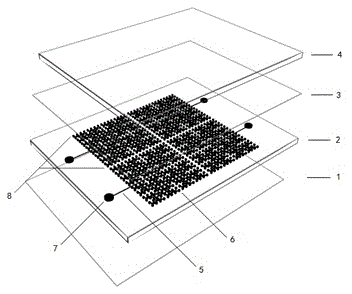
[0063] see figure 1 , the chip of the present invention consists of a cover glass layer (1), a reaction layer (2), a modification layer (3), and a sealing layer (4) sequentially from bottom to top; the reaction layer (2) has four identical Each reaction module (8) is composed of a flow channel (5), a reaction microchamber (6) and an injection port (7); the cover glass layer (1) adopts a cover with a thickness of 0.2mm The slide glass is used as the material, which is pre-treated with air plasma to prepare for combination with the reaction layer (2); the reaction layer (2) is made of polydimethylsiloxane (PDMS), and adopts multilayer soft lithography technology A mold with a microchannel structure is made, and a gas-permeable 5:1 (prepolymer: curing agent) PDMS is poured on the mold to form a cured demoulding; the modification layer (3) is treated with EGC-1720 fluorine surface treatment agent Spin-coating process forms about 10 nm thick nano film with anti-evaporation effect....
Embodiment 2
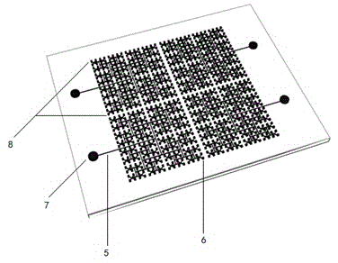
[0065] see figure 2 , is a schematic diagram of the reaction layer (2) of the device of the present invention, wherein (5) is a flow channel, (6) is a reaction chamber, (7) is a sample inlet, and (8) is a reaction module; the reaction module (8) is 4 There are 7 flow channels (5) with a width of 50 μm; the reaction microchamber (6) is a square with a side length of 150 μm and a height of 300 μm.
Embodiment 3
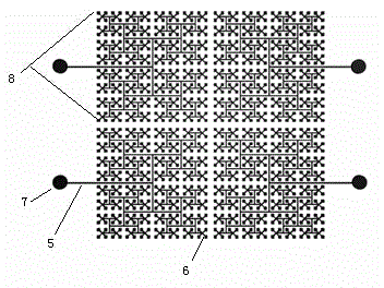
[0067] see image 3 , is a schematic diagram of the design of the reaction layer (2) of the device of the present invention: there are 4 reaction modules (8); the circulation channel (5) has 7 levels, and the width is 30 μm; the reaction microchamber (6) is a square, and the side length is designed is 100 μm, and the height is designed to be 200 μm.
PUM
| Property | Measurement | Unit |
|---|---|---|
| thickness | aaaaa | aaaaa |
Abstract
Description
Claims
Application Information


