

All-solid state electrochromic device preparation method and prepared electrochromic glass
A technology of electrochromic devices and electrochromic glass, which is applied in the fields of instruments, optics, nonlinear optics, etc., to achieve the effect of eliminating the deposition and growth process, avoiding the difficulty of preparation, and improving the electronic insulation performance and ion conductivity
- Summary
- Abstract
- Description
- Claims
- Application Information
AI Technical Summary
Problems solved by technology
Method used
Image

Examples
preparation example Construction
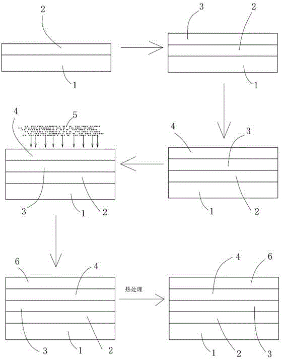
[0022] A preparation method of an all-solid-state electrochromic device (see attached figure 1 ), grow the bottom transparent conductive layer 2 on the transparent substrate 1 by physical vapor deposition, deposit and grow the lower electrochromic layer 3 on the bottom transparent conductive layer, and directly deposit and grow the upper electrochromic layer on the lower electrochromic layer 4. Ion source 5 is deposited on the upper electrode electrochromic layer. The ion source is one or more of lithium, lithium oxide or lithium peroxide. After the ion source is deposited, the top transparent conductive layer 6 is deposited and grown. The top transparent conductive layer After deposition and growth, the device is fabricated by heat treatment or light treatment.
[0023] The ion source deposited on the upper electrode electrochromic layer directly diffuses into the upper electrode electrochromic layer during the deposition process, and the amount of ion source deposited on the...
Embodiment 1
[0028] Embodiment 1: All coatings are completed in a magnetron sputtering system, the underlying transparent conductive layer is made of indium tin oxide (ITO) with a thickness of 300nm, and the cathode electrochromic layer is made of tungsten oxide (WO 3 ), the thickness is 700nm, the anode electrochromic layer is nickel tungsten oxide, the thickness is 320nm, the anode electrochromic layer deposits saturated lithium as the ion source to ionize it, and deposits on the fully ionized nickel tungsten oxide Indium tin oxide (ITO) is the top transparent conductive layer with a thickness of 380nm. After the coating is completed, it is vacuum annealed at 400°C for 30min, and the vacuum degree is 10 -6 torr. The prepared 370mm×470mm electrochromic glass can completely change color within 3 minutes, and the transmittance at 550nm in the visible light region after discoloration is less than 3%, and the transmittance after fading is about 65%.
Embodiment 2
[0029] Example 2: The underlying transparent conductive layer is grown by chemical vapor phase method on fluorine-doped tin oxide (FTO), and the cathodic electrochromic layer tungsten oxide (WO) is grown on it by reactive magnetron sputtering. 3 ), with a thickness of 560nm; reactive magnetron sputtering to grow the anode electrochromic layer nickel aluminum oxide, with a thickness of 280nm; depositing a mixture of lithium oxide and lithium as an ion source, after ionizing the anode electrochromic layer, magnetron sputtering growth Indium tin oxide (ITO) is the top transparent conductive layer; after the coating is completed, it is annealed in the atmosphere at 300°C for 3 hours, and the prepared electrochromic glass of 370mm×470mm can completely change color within 2 minutes, and the 550nm transmittance in the visible light region after color change The rate is less than 3%, and the transmittance after fading is about 65%.
PUM
| Property | Measurement | Unit |
|---|---|---|
| Thickness | aaaaa | aaaaa |
| Thickness | aaaaa | aaaaa |
| Thickness | aaaaa | aaaaa |
Abstract
Description
Claims
Application Information