Longitudinal short-opening grid channel-type HEMT device and preparation method thereof

A grid and vertical technology, which is applied in the field of vertical short-open gate channel HEMT devices and their preparation, can solve the problems of increased device on-resistance, increased electron scattering, and reduced on-current, achieving conduction Effects of reduced resistance, reduced channel resistance, and short open channel

Active Publication Date: 2015-09-16
DALIAN UNIV OF TECH
View PDF3 Cites 11 Cited by
  • Summary
  • Abstract
  • Description
  • Claims
  • Application Information

AI Technical Summary

Problems solved by technology

[0006] The present invention mainly solves the problem of the existing gate structure technical scheme formed by AlGaN barrier layer etching or fluorine ion implantation in normally-off HEMT devices, which respectively cause damage to the 2DEG channel interface used for current transport under the gate and the The increase of electron scattering in the channel leads to the technical problem that the on-resistance of the device becomes larger and the on-current decreases. A new type of vertical short-open gate channel type HEMT device and its preparation method are proposed, which can realize the normally-off type of the device. Large threshold voltage while effectively reducing the on-resistance of the device

Method used


Image

  • Longitudinal short-opening grid channel-type HEMT device and preparation method thereof
  • Longitudinal short-opening grid channel-type HEMT device and preparation method thereof
  • Longitudinal short-opening grid channel-type HEMT device and preparation method thereof

Examples


Embodiment 1

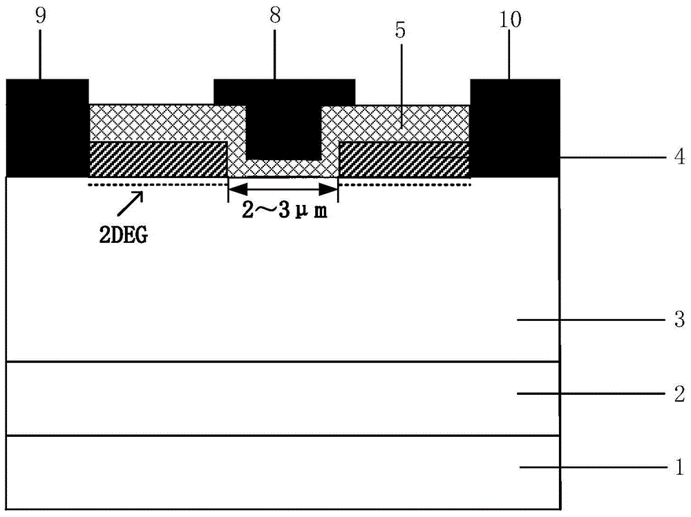
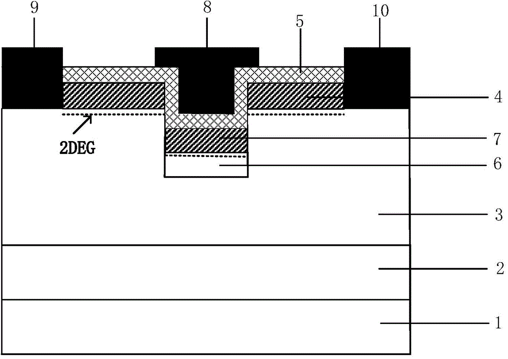
[0050] figure 2 It is a schematic structural diagram of a vertical short open gate channel type HEMT device provided by an embodiment of the present invention. Such as figure 2 As shown, the vertical short open gate channel type HEMT device provided by the embodiment of the present invention includes:

[0051] substrate1;

[0052] a buffer layer 2 on the substrate 1;

[0053] a first GaN layer 3 on the buffer layer 2, the side of the first GaN layer 3 facing away from the buffer layer 2 has a groove;

[0054] The second GaN layer 6 and the second barrier layer 7 embedded in the groove in sequence, wherein the second GaN layer 6 and the second barrier layer 7 form a heterojunction, the interface of which forms a heterointerface, and the heterojunction High density 2DEG at the lateral interface of ;

[0055] The first barrier layer 4 located on the first GaN layer 3 except for the groove, wherein the first GaN layer 3 and the first barrier layer 4 form a heterojunction, a...

Embodiment 2

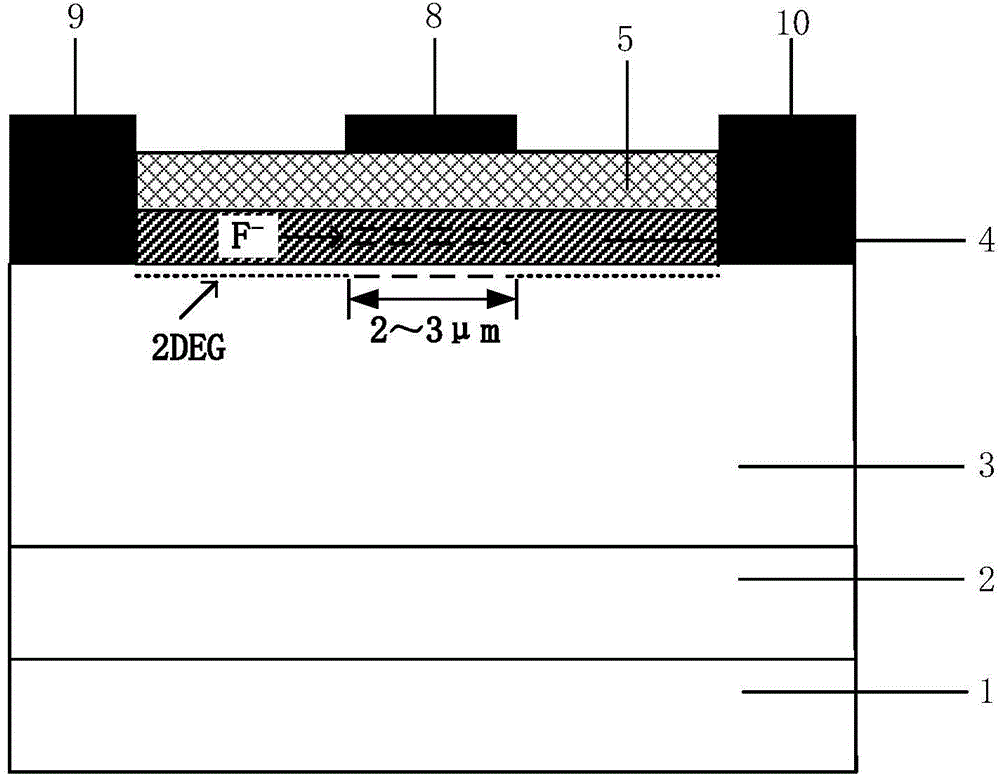
[0066] Figure 4 It is a flow chart for realizing the fabrication method of the vertical short open gate channel type HEMT device provided by the embodiment of the present invention. Such as Figure 4 As shown, the preparation method of the vertical short open gate channel type HEMT device provided by the embodiment of the present invention includes:

[0067] Step 101, forming a laminated structure sequentially composed of a substrate, a buffer layer, a first GaN layer and a first barrier layer.

[0068] Figure 5a It is a structural diagram corresponding to this step of the method for manufacturing a vertically short open gate channel type HEMT device provided by an embodiment of the present invention. refer to Figure 5a , forming a laminated structure consisting of the substrate 1 , the buffer layer 2 , the first GaN layer 3 and the first barrier layer 4 in sequence. The specific process is: providing a substrate 1 ; forming a buffer layer 2 on the substrate 1 ; formin...


PUM


Abstract

The present invention relates to the field of a semiconductor device and provides a longitudinal short-opening grid channel-type HEMT device and a preparation method thereof. The HEMT device comprises a substrate, a buffer layer, a first GaN layer, a second GaN layer, a second barrier layer, a first barrier layer, a dielectric layer, a source electrode, a drain electrode and a grid electrode, wherein the buffer layer is positioned on the substrate; the first GaN layer is positioned on the buffer layer; one side, whic is deviated from the buffer layer, of the first GaN layer is provided with a groove; the second GaN layer and the second barrier layer are sequentially embedded into the groove; the first barrier layer is positioned on the first GaN layer except for the groove; the dielectric layer is positioned on the first barrier layer and the second barrier layer; the source electrode and the drain electrode are in contact with the first GaN layer and the lateral surfaces of the source electrode and the drain electrode are sequentially in contact with the first barrier layer and the dielectric layer from bottom to top; and the grid electrode is in contact with the dielectric layer. According to the present invention, a normally-closed type operation mode of the HEMT device can be obtained; when a large threshold value voltage is realized, on resistance of the device is effectively reduced; and the grid electrode structure also has the characteristics of small capacitor, high switching speed of the device and the like.

Description

technical field [0001] The invention relates to the field of semiconductor devices, in particular to a vertical short open gate channel type HEMT device and a preparation method thereof. Background technique [0002] Power switching devices have broad application prospects in many fields such as renewable energy generation and power system control of military facilities. The performance of traditional silicon-based power devices has approached the theoretical limit of the material. As a typical representative of next-generation wide-bandgap semiconductor materials, gallium nitride (GaN) has the characteristics of large band gap, high critical breakdown electric field, high saturation electron drift rate and good chemical stability. Its heterostructure (represented by AlGaN / GaN) interface has a large density of interface polarization charges, which can induce a high density of two-dimensional electron gas (2DEG) (>10 13 cm -2 ) as a conductive channel, and because the G...

Claims


Application Information

Patent Timeline
Patent Type & Authority Applications(China)
IPC IPC(8): H01L29/778H01L29/10H01L29/423H01L21/335H01L21/28
CPCH01L29/7789H01L29/1033H01L29/401H01L29/4236H01L29/66462
Inventor 黄火林梁红伟夏晓川杜国同
Owner DALIAN UNIV OF TECH
Why Eureka
Try Eureka