Manufacturing method of non-invasive graphene nano-scale device
A nano-device and manufacturing method technology, applied in the field of electron beam lithography, can solve the problem of damaging graphene lattice and so on
- Summary
- Abstract
- Description
- Claims
- Application Information
AI Technical Summary
Problems solved by technology
Method used
Image
Examples
Embodiment 1
[0056] Example 1: Make a 100-200nm wide, 200-500nm period, with a total finger size of 200 μm x 140 μm Stencil, and non-damaging graphene nanodevices fabricated by Stencil lithography:
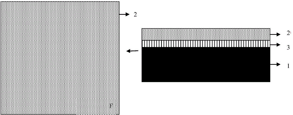
[0057] (1) Use LPCVD to grow 300nm silicon nitride on the silicon substrate. The result is as figure 1 shown.
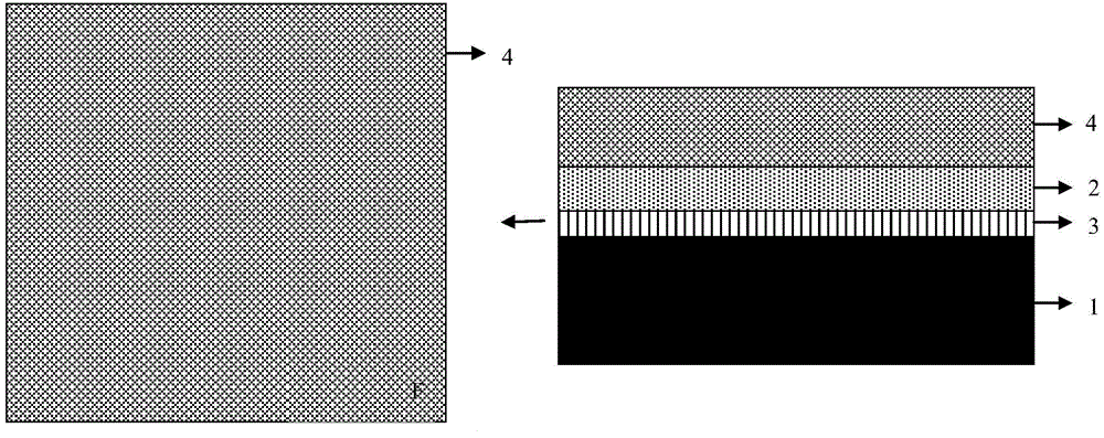
[0058] (2) Spin-coat 300-600 nm PMMA on silicon nitride. The result is as figure 2 shown.
[0059] (3) Bake the spin-coated PMMA silicon wafer in an oven at a temperature of 180°C for 60 minutes or more.
[0060] (4) Measure the thickness of the PMMA glue with a step meter. If the required height is reached, go to (5), otherwise return to step (2).
[0061] (5) Using the above PMMA as a masking layer, design a pattern, expose it by electron beam direct writing, and conduct a dose test.
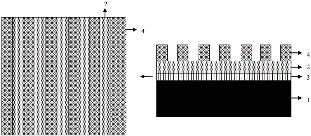
[0062] (6) Develop with developer IMBK and IPA, IMBK:IPA=1:3, developing temperature 23°C, time 1min. The result is as image 3 As indicated, fix with isopropanol for 30 seconds, and ...
PUM
| Property | Measurement | Unit |
|---|---|---|
| Thickness | aaaaa | aaaaa |
Abstract
Description
Claims
Application Information


