TFT ion sensor and TFT ion sensor apparatus using the same

一种离子传感器、离子敏感的技术,应用在测量装置、仪器、科学仪器等方向,能够解决不能提高灵敏度、难检测激素等微量浓度物质等问题

Active Publication Date: 2015-09-30
TIANMA MICRO ELECTRONICS CO LTD
View PDF9 Cites 14 Cited by
  • Summary
  • Abstract
  • Description
  • Claims
  • Application Information

AI Technical Summary

Problems solved by technology

Therefore, in essence, the sensitivity cannot be increased
[0019] It is difficult to detect trace concentrations of substances such as hormones with high precision in related technologies that are constrained by the sensitivity limit based on the Nernst theory

Method used


Image

  • TFT ion sensor and TFT ion sensor apparatus using the same
  • TFT ion sensor and TFT ion sensor apparatus using the same
  • TFT ion sensor and TFT ion sensor apparatus using the same

Examples


Embodiment 1

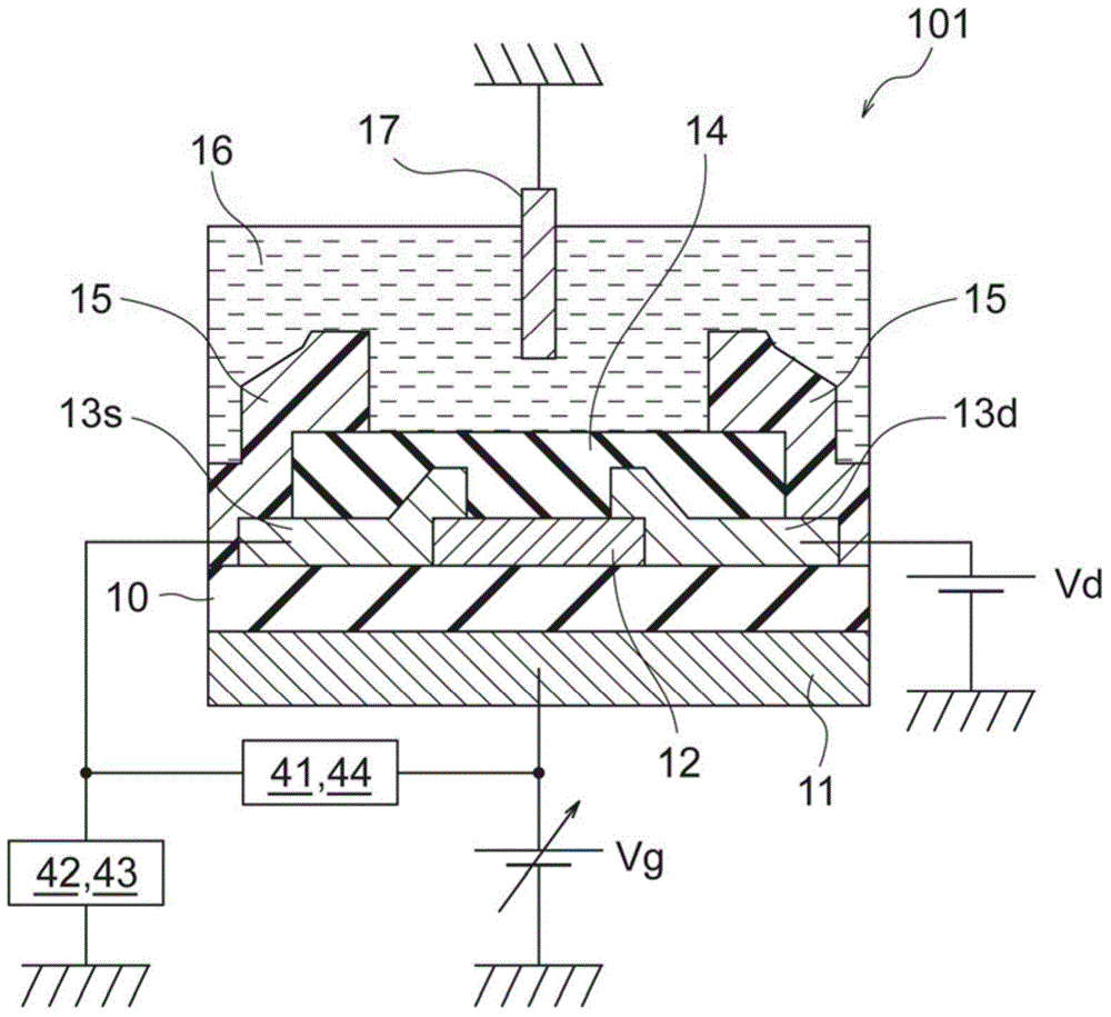
[0053] Next, refer to figure 1 A further concrete example 1 of the first exemplary embodiment will be described.

[0054] First, a silicon substrate 11 on which a 200 nm-thick thermal oxide film 10 is formed is prepared. Instead of the thermal oxide film 10, a silicon oxide film, a silicon nitride film, or the like deposited by a plasma CVD (Chemical Vapor Deposition) method or a sputtering method may be used.

[0055] In addition, a 50-nm-thick oxide semiconductor film made of In—Ga—Zn—O was deposited on the silicon substrate 11 on which the thermally oxidized film 10 was formed by a sputtering method using a metal mask. At this time, a sintered object made of In-Ga-Zn-O was used, and a DC (Direct Current) sputtering method was used in a mixed gas atmosphere of argon and oxygen without heating the substrate. After deposition, it was annealed at 400° C. for one hour. The island-shaped semiconductor active layer 12 is formed by patterning the oxide semiconductor film.

[0...

Embodiment 2

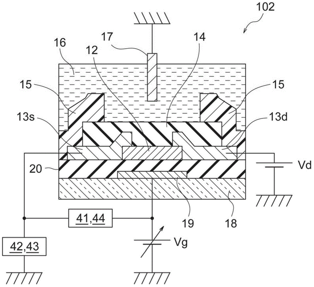
[0076] Next, refer to image 3 Example 2 in which the second exemplary embodiment is further embodied will be described.

[0077] An alloy material mainly composed of aluminum is deposited on the glass substrate 18 by sputtering, and a gate electrode 19 is formed by using a photolithography process including resist coating, exposure, development, etching, and resist stripping.

[0078] Next, a gate insulating film 20 was formed by depositing a 300 nm-thick silicon oxide film at a substrate temperature of 350C by using a plasma CVD method.

[0079] Next, an oxide semiconductor film composed of In—Ga—Zn—O was deposited to a thickness of 30 nm by sputtering, and patterned into a predetermined island shape by a photolithography process to form the semiconductor active layer 12 . After patterning, an annealing treatment was performed at 400° C. for 1 hour in air.

[0080] Then, titanium metal was deposited by sputtering, and after patterning the photoresist, a fluorine-based plas...

Embodiment 3

[0087] (Example 3) Etching stop type IGZO-TFT

[0088] Figure 4 It is a sectional view showing the TFT ion sensor 103 of the third embodiment. refer to Figure 4 Example 3, which is a modified example of the second exemplary embodiment, will be described.

[0089] An alloy material mainly composed of molybdenum is deposited on the glass substrate 18 by sputtering, and the gate electrode 19 is formed by using a photolithography process consisting of resist coating, exposure, development, etching, and resist stripping. .

[0090] Next, by using a plasma CVD method at a substrate temperature of 350° C., a 200-nm-thick silicon nitride film 21 is deposited thereon and a 100-nm-thick silicon oxide film 22 is successively deposited, and their 300-nm-thick laminated film is used as a gate electrode. pole insulating film.

[0091] Next, an oxide semiconductor film 23 composed of In—Sn—Zn—O was deposited to a thickness of 50 nm by sputtering as a semiconductor active layer, and pa...


PUM

PropertyMeasurementUnit
sensitivityaaaaaaaaaa

Abstract

The ion sensors using TFT or MOSFET are low in the measurement sensitivity so that it is difficult to detect an extremely small amount of sensing-target substance. A TFT ion sensor includes both a gate electrode (a silicon substrate) and a reference electrode, in which the electrostatic capacitance of a gate insulating film (a thermal oxide film) is set to be larger than the electrostatic capacitance of an ion sensitive insulating film. Therefore, it is possible to detect the concentration of ions, hormones, and the like in a sensing-target substance from the shift in the threshold voltage of the gate-source voltage to source-drain current property.

Description

[0001] Cross References to Related Applications [0002] This application is based on and claims the benefit of priority from Japanese Patent Application No. 2014-068159 filed on March 28, 2014, which is incorporated herein by reference in its entirety. technical field [0003] The present invention relates to a TFT ion sensor composed of TFT (Thin Film Transistor: thin film transistor), a measurement method using the TFT ion sensor, and a TFT ion sensor device using the TFT ion sensor. Background technique [0004] In recent years, for example, ion concentration sensors for biosensing are utilized in fields such as medical services. The ion concentration sensor is obtained by combining the hydrogen ion concentration detection function on the surface of the inorganic oxide, the oxygen molecule recognition function on the surface of the inorganic oxide with an electrochemical device. [0005] Ion-sensitive FETs (FET ion sensors) using silicon substrate MOSFETs (Metal Oxide ...

Claims


Application Information

Patent Timeline
Patent Type & Authority Applications(China)
IPC IPC(8): G01N27/26
CPCG01N27/414H01L29/7869G01N27/4145G01N27/4148
Inventor 竹知和重芳贺浩史岩松新之辅小林诚也阿部泰矢作彻
Owner TIANMA MICRO ELECTRONICS CO LTD
Why Eureka
Try Eureka